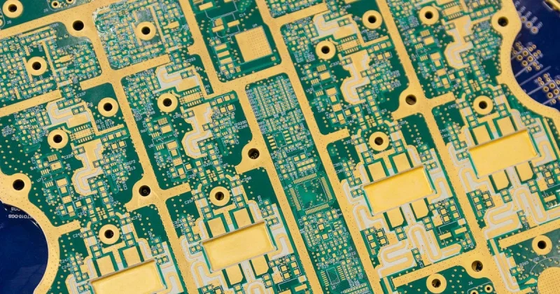
How PCB DFM Impacts Manufacturing and Final Yield
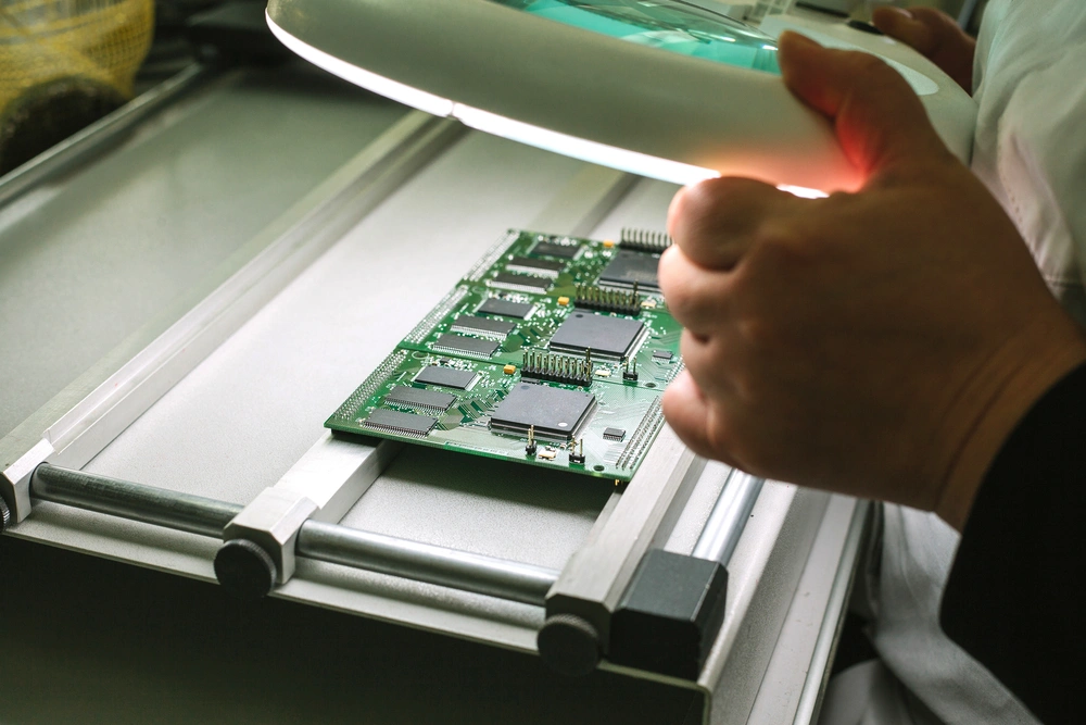
PCB DFM (Design for Manufacturability) is far more than simply checking a few rule boxes in EDA software; it is the digital expression of physical manufacturing boundaries. Many hardware engineers push for extreme electrical performance during the design phase while ignoring the factory’s actual process capabilities, leading to frequent prototype failures and plummeting mass-production yields. The core value of DFM lies in shifting physical manufacturing constraints forward into the design phase. By optimizing trace width, vias, panelization, and copper balance, it directly eliminates potential physical scrap risks. This article provides an in-depth analysis of how DFM rules permeate CAM engineering, bare board fabrication, and SMT assembly, offering an actionable guide to improving yield and reducing costs.
Core Mapping: How DFM Rules Directly Determine Production Yield
The essence of DFM rules is the translation protocol between design intent and manufacturing capability. When design parameters approach or exceed the factory’s physical limits, yield degradation is not linear; it collapses exponentially.
1.1 The 1-10-100 Rule: Exponential Growth of Defect Repair Costs
In the electronics manufacturing industry, defect repair costs strictly follow the “1-10-100 Rule.” If an insufficient trace spacing issue is identified and corrected during the schematic or PCB layout phase (cost of 1), it takes only a few minutes. If the issue flows into CAM engineering or bare board fabrication (cost of 10), it will result in back-and-forth Engineering Queries (EQs), re-panelization, or even the scrapping of an entire batch of laminates. If the defect remains hidden until SMT assembly or end-product testing (cost of 100), it triggers component damage, rework, desoldering, or even massive product recalls. The primary task of DFM is to intercept over 90% of potential defects in the design phase, where the cost is “1.”
1.2 Process Window and the Mathematical Relationship with DFM Tolerances
The process window refers to the allowable parameter fluctuation range within which manufacturing equipment can stably produce qualified products. A high-yield DFM design must ensure that design tolerances fall entirely within the manufacturing process window, leaving a safety margin.
The mathematical relationship can be simplified as: Design Limit = Factory Process Limit × (1 + Safety Margin).
For example, if a fab’s standard minimum trace width limit is 0.15 mm (6 mil), and the designer sets a 20% safety margin, the minimum trace width in the DFM rules should be set to 0.18 mm (approx. 7 mil). This mathematical concession effectively absorbs uncontrollable process noise, such as fluctuations in etchant concentration and exposure alignment deviations, pushing yields from 85% to over 99%.
1.3 Engineering Trade-offs: Extreme Electrical Performance vs. High Manufacturing Yield
In high-speed and high-frequency board design, engineers often compress trace widths and spacing to the process limit to achieve precise 50Ω/100Ω differential impedance. However, extreme electrical performance is often mutually exclusive with high manufacturing yield. Mature DFM decision-making is not about blind compromise. Instead, it involves optimizing the stack-up (such as adjusting prepreg thickness) or switching to low-Dk/Df high-frequency laminates. This allows designers to relax trace width and spacing (improving yield) while still meeting signal integrity (SI) requirements. This engineering trade-off is the core dividing line between senior hardware designers and junior layout engineers.
Front-End Engineering and CAM: How DFM Affects Lead Times and Engineering Communication
Once design files (Gerber/ODB++) are submitted, the review efficiency of CAM engineers directly determines the project’s NPI (New Product Introduction) lead time. Excellent DFM design makes CAM processing seamless, while poor design traps the project in an endless cycle of EQs.
2.1 CAM Engineering Review Process and SOP for Efficient EQ Communication
When a design contains ambiguities or conflicts, the fab will issue an EQ. To shorten lead times, it is recommended to follow this efficient communication SOP:
- Preventive Notes: In the Gerber Readme file, clearly specify impedance control layers, special hole metallization requirements, and panelization intent.
- EQ Graded Response: Categorize EQs into “Fatal Blockers” (e.g., minimum hole size smaller than the drill limit) and “Optimization Suggestions” (e.g., suggesting larger via pads). Immediately modify source files for fatal issues, and quickly authorize optimization suggestions after evaluation.
- Closed-Loop Confirmation: All EQ replies must be documented through the official engineering system to avoid version control errors caused by verbal agreements or instant messaging.
2.2 The Decisive Role of Panelization in Material Utilization and SMT Efficiency
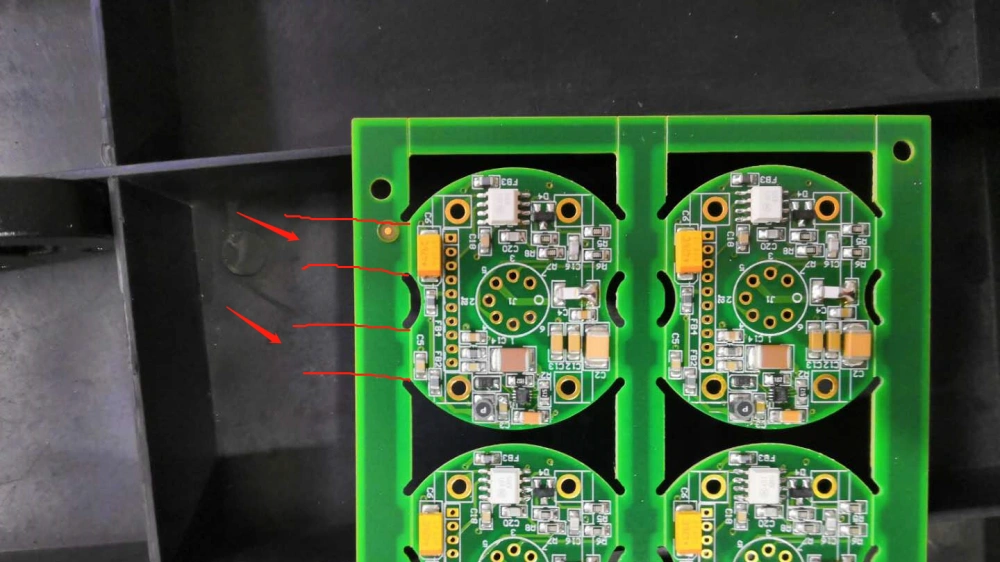
Running single, small PCBs directly through an SMT line results in a high empty-load rate on the conveyor rails and frequent changeovers. Panelization combines multiple small boards into a standard size (e.g., 250×330 mm) large panel, directly doubling placement efficiency. When it comes to panel connection methods, the choice between V-Cut and Tab Routing is critical.
Comparison Dimension | V-Cut (V-Groove) | Tab Routing | Selection and DFM Guidelines |
Applicable Shapes | Regular rectangular boards connected by straight lines | Circular, irregular, or boards with internal routed slots | Prioritize V-Cut for regular boards; Tab Routing is mandatory for irregular shapes. |
Separation Method & Stress | Snapped along the V-groove; stress is relatively concentrated | Milled connection points; prone to residual burrs after separation | Place tab routing points closer to the inner side of the board to prevent burrs from affecting assembly. |
Stress & Deformation Control | Overall rigidity decreases after cutting | Uneven tabs can cause thermal deformation during reflow soldering | Tab routing connections must be evenly distributed around the perimeter of the panel. |
Clearance Requirements | Traces/pads must be ≥0.4 mm (16 mil) from the V-Cut edge | Limited by milling cutter radius; inner corners require fillets to prevent stress concentration | Strictly prohibit routing traces or placing pads on the V-Cut line to prevent trace breakage during depaneling. |
2.3 How to Efficiently Interpret DFM Reports: Distinguishing “Must-Fix” from “Should-Fix”
Professional PCB manufacturers provide DFM reports that typically include dozens of checks. Engineers must know how to prioritize:
- Must Fix: Issues such as trace widths below 0.1 mm (exceeding factory capabilities), via annular rings smaller than 0.127 mm (the IPC-2221 lower limit), or V-Cut lengths under 7 mm (equipment limit). Failing to correct these will directly result in physical scrap and must be rectified unconditionally.
- Should Fix: Suggestions like increasing a 0.3 mm trace to 0.5 mm to improve current-carrying margin, or adding test coupons. These can be decided flexibly based on product positioning and budget.
Bare Board Fabrication: Causal Analysis of DFM Design Flaws and Physical Scrap
Bare board fabrication involves dozens of chemical and physical processes. Minor flaws in DFM design are infinitely amplified during these processes, ultimately leading to the scrapping of the entire board.
3.1 Impact of Trace Width/Spacing and Via Design on Etching and Drilling Yields
- Etching Compensation and Spacing: The etching process suffers from the undercut effect. If the designed trace spacing is tight against the 0.15 mm limit, the actual spacing after etching may increase due to undercut, but the trace width will thin out, leading to impedance shifts or even open circuits. DFM requires that standard power traces on 1 oz copper foil be ≥0.3 mm (12 mil) to balance current capacity and etching yield.
- Drill Wander and Annular Rings: During multi-layer board drilling, slight vibrations of the drill bit cause hole position deviations. If the via annular ring is designed too small, this deviation will directly cause a “90-degree breakout” (partial disconnection of the hole ring). DFM rules must ensure the annular ring width is at least 0.05 mm larger than the factory’s minimum tolerance limit.
3.2 The Fatal Impact of Copper Balance and Thermal Management on Board Warpage
PCB warpage is a nightmare during the SMT phase, causing uneven solder paste printing and component open joints. The root cause of warpage is the mismatch in the Coefficient of Thermal Expansion (CTE) between interlayer materials and the uneven release of thermal stress.
- Copper Area Balance: A massive difference in copper area between the outer Component (top) and Solder (bottom) layers causes asymmetric stress during lamination and baking. DFM requires the copper pour area on the top and bottom layers to be as close as possible; large copper-free areas must be filled with copper grids.
- Baking for Stress Relief: On the manufacturing side, laminates must be baked at 150°C for 3 hours before cutting to remove moisture and cure the resin. If the symmetrical arrangement of interlayer prepregs is not considered during design, factory baking cannot completely eliminate internal stress.
3.3 Top 3 Common Fatal Defects: Acid Traps, Annular Ring Breakout, and Solder Mask Bridge Peeling
- Acid Traps: Two traces intersect at an acute angle of less than 45 degrees. Etchant tends to pool at the sharp corner, leading to over-etching or open circuits. Prevention: DFM rules must enforce an “avoid acute angles” check; all trace angles must be ≥45 degrees or use curved routing.
- Annular Ring Breakout: Caused by drill wander or undersized pads, as mentioned above. Prevention: Calculate via hole tolerances at ±0.05 mm, and ensure the pad diameter is at least 0.25 mm larger than the hole size.
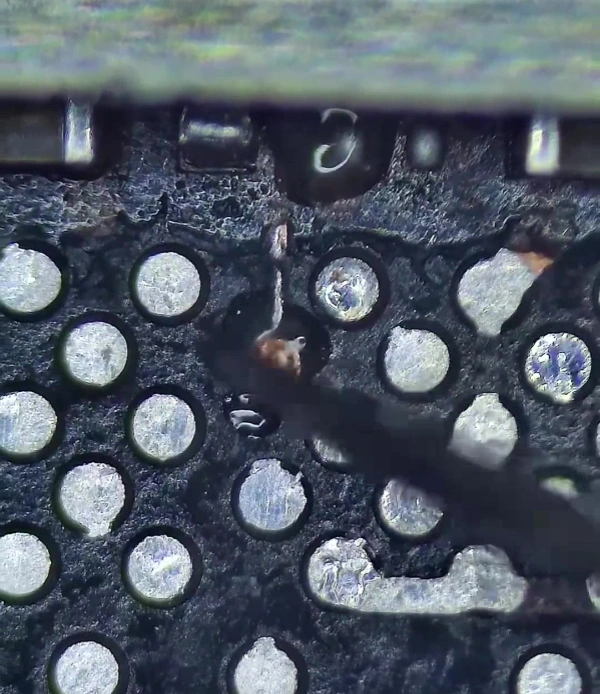
- Solder Mask Bridge Peeling: The solder mask bridge between BGA or fine-pitch IC pads is too narrow (<0.1 mm) and peels off during development or the thermal shock of soldering, causing short circuits. Prevention: If trace spacing cannot be increased, use a Solder Mask Defined (SMD) pad design, abandoning the solder mask bridge and relying on precise stencil apertures to control solder paste volume.
SMT Assembly: Ensuring Soldering Yield Through DFM and DFA Synergy
Completing bare board fabrication is only the first step. Soldering yield during the SMT (Surface Mount Technology) phase is equally dependent on the early synergy between DFM and DFA (Design for Assembly).
4.1 Component Placement and Pad Design to Prevent Tombstoning and Cold Solder Joints
Small package components like 0402/0201 are highly susceptible to “tombstoning” after reflow soldering. The root cause is asymmetric thermal mass at the two ends of the component pads, causing the solder paste on one end to melt first, pulling the component upright via surface tension.
- DFM Countermeasures: Ensure the pad dimensions at both ends are completely identical. The traces connecting to the pads must be symmetrical to avoid connecting one end to a large copper pour (which dissipates heat quickly) and the other to a thin trace (which dissipates heat slowly). If connecting to a large copper area is unavoidable, design thermal reliefs or extend the trace length.
- Misalignment Control: Non-standard pad designs can cause placement misalignment rates to exceed 20%. Pad sizes and spacing must strictly match the component datasheet and IPC-7351 standards, while also accommodating the visual recognition accuracy of the SMT pick-and-place machine.
4.2 Differentiated DFM Review Strategies for Special Processes
- HDI Boards: Involves blind/buried vias and laser drilling. Minimum trace widths can reach 0.075 mm (3 mil). DFM must focus on reviewing the microvia hole-to-pad ratio (cap-on-pad) and employ resin-filled and capped vias (POFV) to prevent solder paste from flowing into the holes during SMT, which causes open joints.
- High-Frequency Boards: Substrates (like Rogers) are relatively soft with weak copper adhesion. DFM must avoid large areas of isolated copper, add mechanical mounting holes, and strictly control etching undercut to ensure impedance consistency.
- Heavy Copper Boards (≥2 oz): Etching is extremely difficult, requiring significantly wider trace spacing. DFM must employ “teardrop” designs to strengthen the connection between vias and traces, preventing breakage under thermal shock.
4.3 Defining Boundaries and Synergistic Optimization Between DFM and DFA
DFM focuses on “whether the board can be manufactured,” while DFA focuses on “whether components can be assembled well and inserted quickly by manual labor.” Their synergy is reflected in:
- Through-Hole Component Hole Sizes: DFA requires pins to insert smoothly, while DFM requires good hole wall plating. The best practice is to make the hole diameter 0.1 to 0.2 mm larger than the pin diameter. This ensures smooth assembly and good capillary action during wave soldering to prevent missed solder joints.
- Panelization Process Edges: DFA needs to consider SMT rail clamping (typically requiring a 5 mm margin), while DFM needs to consider the strength of V-Cuts or tab routing. A synergistic optimization is to use “dummy panelization” or breakaway process edges, adding fiducial marks and optical tooling holes on the process edges.
Commercial Translation and Implementation: DFM Quantitative ROI Model and Core Checklist
DFM is not just technical work; it is a business decision. Quantifying the cost reductions brought by DFM can effectively drive collaboration between R&D and the supply chain.
5.1 DFM Cost Reduction Calculation Model and ROI Analysis
Take panel gap optimization as an example: Traditional designs use a 5 mm process edge for standard panelization, resulting in larger panel sizes. If optimized through DFM by using right-angle V-Cut splicing and compressing the gap to 0.3 mm, the panel size can be significantly reduced.
- Material Cost: Laminate utilization increases from 70% to over 85%, reducing the material cost per PCB by about 12%.
- Manufacturing Cost: Waste liquid treatment volume decreases, and drilling/routing time is shortened.
- SMT Cost: The number of PCBs passing through the reflow oven per unit of time increases, reducing equipment depreciation and labor allocation costs by 15%-20%.
Comprehensively calculated, a deep DFM optimization on a mass-production order of 100,000 units can typically save over 15% in total manufacturing costs, yielding a highly favorable ROI.
5.2 Standard Supply Chain Collaboration SOP: Design – DFM Review – Prototyping – Mass Production
- Design Phase: Engineers import the fab’s “Process Capability Specification” and configure the DFM rules in the EDA software.
- DFM Review Phase: After exporting Gerbers, use third-party DFM software (like Valor) or submit to the fab for automated and manual dual reviews.
- Prototyping Verification Phase: For “Should Fix” items in the DFM report, conduct A/B testing during prototyping (e.g., testing the impact of different trace widths on temperature rise).
- Mass Production Freeze Phase: Solidify the verified DFM parameters into the company’s standard Design Guidelines, forming organizational assets.
5.3 20-Item Core DFM Review Checklist from a Manufacturer’s Perspective
To ensure a flawless design, verify the following 20 core metrics before releasing the board for fabrication:
Trace Width/Spacing and Routing (5 Items)
- Is the minimum trace width/spacing greater than the factory’s standard limit (recommended ≥0.15 mm / 6 mil)?
- Do power trace widths meet current-carrying requirements (recommended ≥0.3 mm for 1 oz copper)?
- Are all trace angles ≥45 degrees or curved, with no acute acid traps?
- Are differential traces strictly matched in length and spacing, avoiding crossing split planes?
- Are inner layer traces increased by 20-50% compared to outer layers to compensate for poorer heat dissipation?
Vias and Pads (5 Items)
- Is the via annular ring width ≥0.127 mm (meeting IPC-2221 standards)?
- Are vias in BGA areas processed with resin-filled and capped (POFV) technology?
- Are through-hole diameters 0.1 to 0.2 mm larger than the component pins?
- Are test point diameters ≥0.8 mm with a spacing of ≥1.27 mm?
- Do high-current vias use a parallel array of multiple small holes rather than a single large hole?
Panelization and V-Cut/Tab Routing (5 Items)
- Is there a strict safety clearance of ≥0.4 mm (16 mil) between V-Cut traces/pads and the cutting edge?
- Is the minimum effective V-Cut length ≥7 mm?
- Are tab routing connections evenly distributed around the panel perimeter to prevent deformation?
- Is there at least a 5 mm SMT rail clamping margin reserved on the panelization process edges?
- Is the overall panel size within the standard range (e.g., 250×330 mm) with a reasonable aspect ratio?
Solder Mask, Silkscreen, and Thermal Management (5 Items)
- Is the solder mask bridge width between fine-pitch ICs/BGAs ≥0.1 mm, or changed to SMD if not?
- Is silkscreen text kept off the pads (strictly prohibited on pads, as it affects soldering)?
- Is the copper area balanced between the top and bottom layers, with large copper-free areas filled with grids?
- Are thermal via arrays added beneath heat-generating components?
- Is there sufficient keep-out area reserved around mounting holes to prevent screws from crushing traces?
Core Technical FAQ: Resolving PCB DFM Engineering Practice Questions
Q1: What is DFM, and why is the first step in setting PCB design rules to consult the fab’s “Process Capability Specification”?
A: DFM (Design for Manufacturability) translates physical manufacturing constraints into rules within design software. Consulting the Process Capability Specification first is crucial because equipment precision (like laser drill sizes or minimum spacing) varies drastically between factories. Discussing DFM rules without considering a specific factory’s capabilities is like setting a car’s speed limit without looking at the road conditions—it inevitably leads to unmanufacturable designs or out-of-control yields.
Q2: Why must single PCBs be panelized into large arrays for SMT assembly when they can technically be manufactured individually?
A: SMT line equipment (pick-and-place machines, reflow ovens, AOI) calculates costs based on “processing capacity per unit of time.” Running single small boards through the oven results in a high empty-load rate on the conveyor rails, and frequent changeovers waste massive amounts of time. After panelization, the equipment processes 8 or even 16 boards at once, doubling efficiency and significantly driving down the manufacturing cost allocated to each individual PCBA.
Q3: What are the three absolute “hard prohibitions” in V-Cut design?
A: 1. Traces/pads tight against the cut line: A 0.4 mm safety clearance must be maintained; otherwise, the mechanical stress of depaneling will snap traces or rip off pads. 2. V-Cutting through routed slots: This drastically reduces the width of the connecting tabs, causing the panel to break prematurely during SMT reflow. 3. Cut length less than 7 mm: This falls below the process limit of V-Cut equipment, preventing the blade from cutting properly.
Q4: How can we prevent bridging and tombstoning of small package components like 0402/0201 after reflow soldering during the DFM phase?
A: Tombstoning is primarily caused by asymmetric thermal mass at the two ends of the component pads. During the DFM phase, ensure that the pad dimensions at both ends are identical and that the traces connecting to the pads are symmetrical. Avoid routing one end to a large copper pour (which dissipates heat quickly) and the other to a thin trace. If connecting to a large copper area is unavoidable, use thermal reliefs or extend the trace length to balance the heat dissipation.
For a production-ready design review, connect these DFM rules with the PCB Design engineering service before fabrication.
Table of Contents
- Lập bản đồ lõi: Quy tắc DFM ảnh hưởng trực tiếp đến năng suất sản xuất như thế nào
- Kỹ thuật Front-End và CAM: DFM ảnh hưởng đến thời gian sản xuất và giao tiếp kỹ thuật như thế nào
- Gia công mạch in trần: Phân tích nguyên nhân các lỗi thiết kế DFM và phế phẩm vật lý
- Lắp ráp SMT: Đảm bảo hiệu suất hàn thông qua sự phối hợp giữa DFM và DFA
- Dịch thuật và triển khai thương mại: Mô hình ROI định lượng DFM và danh sách kiểm tra cốt lõi
- Câu hỏi thường gặp về kỹ thuật cốt lõi: Giải đáp các câu hỏi về thực tiễn kỹ thuật thiết kế PCB DFM
Tags
Related Posts
PCBA Prototype
September 8, 2026

PCBA Prototype
August 7, 2026