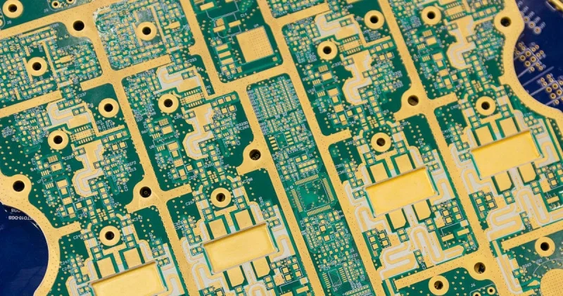
AI Accelerator PCB Design: Signal, Power & Thermal Design
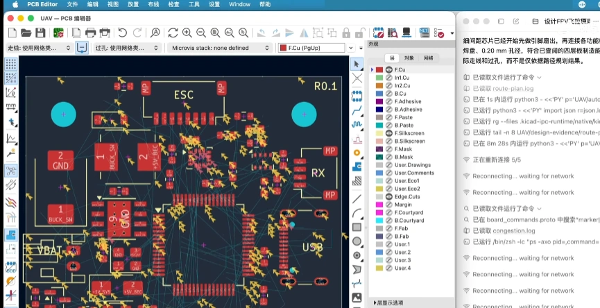
AI accelerator PCB design determines how a board or board assembly connects, powers, cools, and tests a GPU, AI ASIC, or accelerator module inside a server. Its defining challenge is not simply density. It is the interaction of high-speed channels, large and rapidly changing currents, heat removal, mechanical loading, and manufacturability.
Modern accelerator platforms combine high-bandwidth compute devices, dense memory, inter-accelerator links, server I/O, and increasingly demanding cooling. NVIDIA's Blackwell architecture and AMD's Instinct MI300 series illustrate the direction: more memory bandwidth and more tightly integrated multi-accelerator systems. At PCB level, that direction turns electrical, thermal, and manufacturing choices into a coupled engineering problem.
The practical sequence is:
AI accelerator or GPU/ASIC -> high-speed and high-current interfaces -> stack-up and power-delivery architecture -> signal, power, and thermal integrity -> fabrication and assembly controls.
Treating those stages as separate handoffs is a common source of late layout changes, marginal channel performance, VRM instability, warped assemblies, and low first-pass yield.
What is an AI accelerator PCB?
An AI accelerator PCB is a high-density printed circuit board used in an accelerator card, accelerator module carrier, server baseboard, switch board, or similar compute assembly. It distributes power, provides controlled-impedance paths for board-level interfaces, carries support circuits and connectors, and forms part of the thermal and mechanical system.
It is important to define the board boundary before setting rules. A PCIe add-in card, an OAM-style accelerator module, a GPU baseboard, and a server motherboard place different functions on the PCB. They may all be called an "AI accelerator board," but they do not have the same layer count, via structure, material set, cooling arrangement, or test strategy.
| Board context | PCB role | Dominant design tension |
|---|---|---|
| Accelerator add-in card | Hosts an accelerator package, local power conversion, edge connector, and supporting I/O | Dense package escape, host interface channel, local PDN, and heat-sink mechanics |
| Accelerator module or carrier | Connects a compute module to power, fabric, server I/O, and cooling hardware | High pin count, module connector behavior, current delivery, and mechanical flatness |
| Server baseboard or motherboard | Connects CPUs, accelerator modules or slots, networking, storage, and management | Many long channels, connector transitions, reference continuity, and system-level power distribution |
| Switch or fabric board | Routes high-speed links between accelerators, switches, or network devices | Channel loss, crosstalk, return-path integrity, and connector/cable transitions |
Why do AI accelerator boards require high-layer-count PCBs?
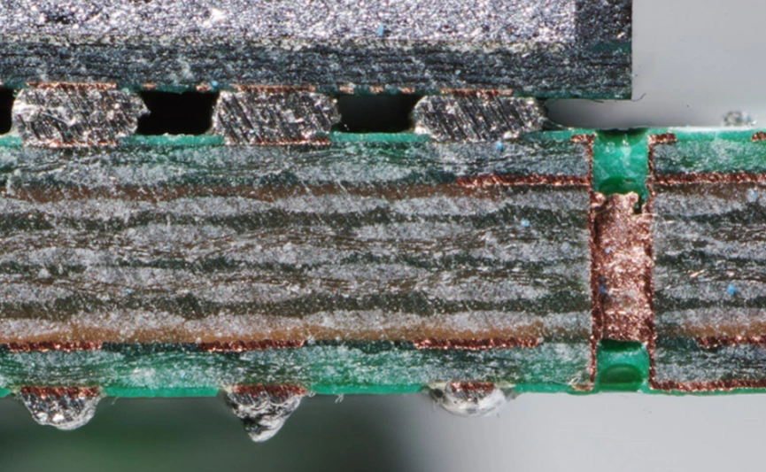
AI accelerator boards often need more layers because they need several independent routing, reference, power, and thermal functions in the same footprint. More layers are useful only when the stack-up assigns each function deliberately.
Dense BGA escape, high lane counts, power and ground distribution, and connector breakout consume routing area quickly. Additional layers can keep critical high-speed routes adjacent to continuous reference planes, provide nearby plane pairs for low-inductance power delivery, separate noisy converter regions from sensitive clocks or management signals, and preserve space for thermal and mechanical features.
Layer count alone does not solve signal integrity. A stack-up with extra routing layers but poor reference-plane adjacency can still create discontinuous return paths and difficult via transitions. Conversely, a lower-layer-count board can be appropriate when its actual channel count, package escape, power demand, and loss budget permit it. The decision should come from the interface topology and the approved fabrication stack-up, not from a fixed layer-count target.
For stack-up fundamentals, see GreatPCB's PCB stack-up design guide. For dense escape routing, HDI PCB construction is relevant when the package pitch, routing density, and fabrication process justify it.
How high-speed signaling changes stack-up and material selection
At AI-server data rates, a trace is a transmission line. Its geometry, dielectric environment, copper surface, vias, connectors, and return path determine whether the receiver gets a usable signal.
Board-level interfaces may include PCIe, Ethernet or InfiniBand-class networking, accelerator-to-accelerator interconnects, clocking, and management links. These must be distinguished from signals that remain inside an accelerator package. In a board channel, the designer has to control the entire path, not just the trace width on one layer.
Insertion loss, return loss, impedance, and crosstalk
| Term | What it describes | Board-level cause | Design consequence |
|---|---|---|---|
| Controlled impedance | The transmission-line impedance set by trace geometry and its reference structure | Trace width, copper thickness, dielectric thickness, solder mask, and nearby copper | A nominal width is not enough; the fabricator's actual stack-up must be used in the field-solver model |
| Return loss | Energy reflected toward the source by an impedance discontinuity | Via transitions, connector launches, plane changes, stubs, pad geometry, or abrupt width changes | A route can meet its nominal impedance yet have poor local transitions |
| Insertion loss | Signal attenuation from source to receiver | Dielectric loss, conductor loss and roughness, vias, connectors, and path length | A longer or rougher channel can close the margin even when reflections are controlled |
| Crosstalk | Unwanted coupling between adjacent signals | Parallel routing, inadequate spacing, shared discontinuous references, or dense breakouts | Victim noise and timing uncertainty rise as coupling and edge rate increase |
The material question therefore begins with a channel budget, not with a brand name. Standard FR-4 constructions may be suitable for some paths. Other paths may need a lower-loss resin system or copper foil treatment because their length, frequency content, connectors, and required margin make loss the limiting factor. The material selection also has to consider resin flow, glass weave effects, thermal behavior, drill quality, availability, and the intended assembly cycle. GreatPCB's PCB raw-materials overview provides background on the main board-material categories.
GreatPCB's controlled-impedance primer explains why impedance discontinuities cause reflections, while its insertion-loss guide provides useful background on loss mechanisms. For an accelerator program, extend that analysis through the package escape, via field, connectors, cables, and receiving device, using the interface owner's current design rules and models.
Build the stack-up around reference continuity
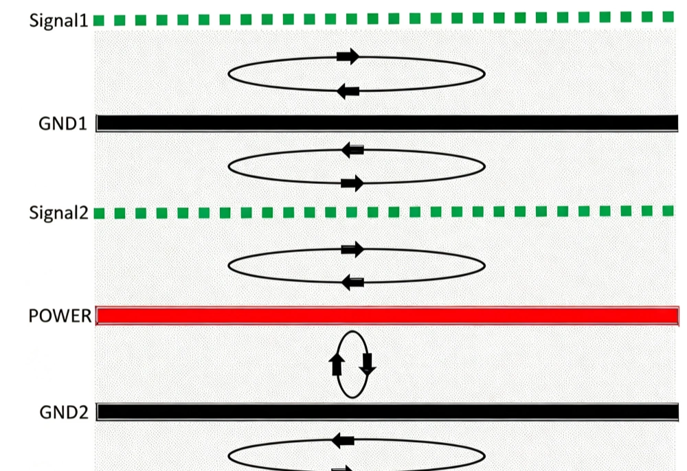
Critical differential pairs and clocks should run near a solid, intended reference plane. Their return current follows the electromagnetic field, so a plane split, anti-pad transition, or reference change can create an impedance discontinuity and enlarge the return loop. When a signal changes layers, the transition needs an intentional return path, often through nearby reference vias or another defined structure.
Do not put high-speed layers beside power or ground planes by habit alone. Confirm the resulting impedance, plane capacitance, fabrication tolerance, and escape-routing feasibility with the board supplier. A stack-up that is electrically attractive but has impractical dielectric thicknesses, copper distribution, or sequential-lamination requirements is not a production stack-up.
How does HBM affect PCB design?
HBM usually affects an AI accelerator PCB indirectly. The high-bandwidth connection between the processor and HBM stacks is normally built inside the advanced package, through package-level interconnect such as an interposer or substrate; it is not routed as ordinary PCB traces.
JEDEC's HBM3 standard, JESD238B.01, defines an HBM DRAM interface. Accelerator products may use HBM in different package implementations, so designers should obtain the actual module, package, and interface documentation rather than assume one topology.
HBM still changes the board in several important ways:
- An HBM-equipped accelerator package or module becomes a large, high-power, high-pin-count assembly with strict escape, flatness, and thermal constraints.
- The board must support the package's power-delivery network and decoupling strategy without forcing high-current paths through narrow neck-downs or sparse via fields.
- Dense package and module geometry competes for the same board area needed by VRMs, connectors, fabric links, management circuits, and cooling hardware.
- HBM increases the need to distinguish package-level memory routes from board-level interfaces such as PCIe, networking, or accelerator fabric links. Applying board-length routing rules to HBM die connections is a category error.
This distinction is useful in design reviews: ask which connections are package-controlled, which are module-controlled, and which are true PCB channels. Each has different ownership, models, and verification methods.
Why signal integrity is central to AI accelerator PCB design
Signal integrity matters because an accelerator board carries interfaces whose margin is shared by the package, PCB, connectors, cables, and receiver. Loss or reflection at any one transition consumes margin from the complete channel.
The SI workflow should start before placement is fixed:
- List every critical interface, its topology, reference clocking, allowable channel components, and source/receiver design guide.
- Allocate a loss and discontinuity budget across package escape, PCB route, vias, connectors, and any cable or backplane path.
- Lock the relevant dielectric constructions, copper types, impedance targets, and allowable fabrication tolerances with the fabricator.
- Simulate or otherwise verify the full channel with the models approved for that interface.
- Preserve the assumptions in release notes and change control. A laminate, connector, via treatment, or stack-up substitution can invalidate an earlier model.
The layout details are not cosmetic. Long unbroken parallel runs increase coupling; stubs can create resonances; connector launches can dominate an otherwise well-routed channel; and a lane that crosses a split reference has a disrupted return path. When possible, design the topology to avoid unnecessary transitions first, then optimize unavoidable discontinuities with the relevant simulation and test data.
How high power density changes power delivery and VRM layout
AI accelerator power density turns the PCB into part of the power-delivery network (PDN). The board must carry high current with low resistance and low inductance while keeping voltage ripple and transient droop within the accelerator's requirements.
The accelerator, voltage-regulator modules, decoupling capacitors, connectors, and planes form one PDN. A wide copper pour may have low DC resistance but still have excessive inductance if the current loop is large or the path changes layers inefficiently. A local capacitor helps only when its placement and connection inductance allow it to respond in the frequency range where it is needed.
Practical power-layout decisions include:
- Place VRM phases and their input/output capacitors according to the regulator and package guidance, with short, symmetric high-current loops where the topology requires them.
- Use continuous power and ground planes or pours with enough parallel via connections at layer changes. Check the complete path through connector contacts, copper neck-downs, vias, solder joints, shunts, and module contacts.
- Partition high di/dt switching loops from sensitive clocks, reference supplies, high-speed lanes, and low-level management or sensing circuits.
- Treat decoupling as a frequency-dependent network, not a capacitor count. Package capacitors, local board capacitors, plane capacitance, and bulk energy storage perform different roles.
- Verify current sharing and heating near via arrays, thermal pads, connectors, and plane voids. These often become the real bottlenecks after a broad top-layer pour has been added.
GreatPCB's power PCB layout article is a useful starting point for power-component placement and multilayer distribution. Accelerator PDN design then needs the device vendor's power targets and package models; no generic copper weight or capacitor recipe is adequate for every GPU or AI ASIC.
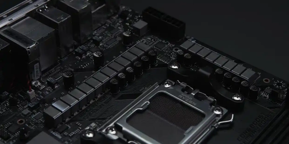
GreatPCB supports complex, high-layer-count PCBs for AI accelerator, server, and high-speed applications worldwide.
Thermal management is a PCB, package, and mechanical problem
Thermal performance depends on the complete path from the accelerator, VRMs, nearby support circuits, and other hot components to the heat sink, cold plate, airflow, or chassis. Copper alone cannot replace a defined mechanical cooling path.
AI server hardware commonly places high heat flux near dense electrical interconnect. The PCB must therefore support the cooling assembly while avoiding new reliability risks. Local copper spreading, thermal vias, package land patterns, component spacing, board thickness, stiffeners, fasteners, and keep-out zones all affect the result.
Key checks include:
- Map losses and hot spots in the actual operating configuration, including the intended airflow or liquid-cooling hardware.
- Keep temperature-sensitive components and references away from switch-node coupling and from the thermal plume of power stages.
- Review via-in-pad, filled-via, solder-mask, and stencil decisions together for thermal pads. The design needs a process that controls solder wicking and voiding where those effects matter.
- Assess board bow and twist, connector coplanarity, heat-sink loading, and module retention. A mechanically stressed board can create intermittent connector or BGA failures even if the electrical layout is sound.
- Consider the laminate's thermal and mechanical behavior, including z-axis expansion and glass/resin construction, alongside the assembly profile and expected operating environment.
Thermal design also feeds back into SI and PI. A thicker copper choice may improve spreading or DC loss but changes impedance. A heat sink or cold plate may impose keep-outs that lengthen a high-speed path. Moving a VRM can reduce a thermal peak while increasing PDN inductance. These are co-design trade-offs, not independent optimizations.
EMC and EMI: control fields and return paths early
Accelerator boards create both high-frequency signal fields and fast switching-power fields. EMC control begins with stack-up, placement, and return-path continuity; shielding or filtering added after layout has limited ability to repair a noisy current loop.
Keep high-speed routes over continuous references, avoid unnecessary plane splits, and make layer transitions return-aware. Keep regulator switch nodes and gate-drive loops compact. Separate them from sensitive reference circuits and high-speed lanes, and provide a clear intended return path for every interface.
At server boundaries, connector selection, chassis bonding, cable shield termination, common-mode behavior, and enclosure geometry can matter as much as a local trace. Board-level EMC review should include the actual module, cable, heat sink, chassis, and cooling configuration rather than only an isolated bare board.
PCB manufacturing and assembly challenges for AI accelerator boards
The manufacturing challenge is not simply making finer features. It is reproducing the electrical, thermal, and mechanical assumptions of a dense design across production lots.
High-layer-count boards add registration, drilling, plating, and material-control complexity. HDI constructions may also require sequential lamination and controlled microvia structures. Fine-pitch package escapes may require filled-and-capped vias or carefully designed via fields. Long high-speed channels may require stub management or back-drilling where the design and fabrication capability support it. These choices can increase yield risk, cost, and inspection needs, so they should be justified by the actual interface and routing problem.
| Manufacturing area | What must be agreed before release | Failure risk when it is left implicit |
|---|---|---|
| Stack-up and materials | Dielectric build, copper types and weights, loss-related material data, impedance requirements, and allowed alternates | The built board no longer matches the modeled channel or PDN |
| HDI and via structure | Laser/mechanical drill strategy, sequential lamination, via filling/capping, aspect-ratio limits, registration, and coupon needs | Opens, weak interconnects, breakout loss, warpage, or poor yield |
| High-current copper | Finished copper, etch compensation, plane voids, thermal relief strategy, via arrays, and connector transitions | Local heating, voltage drop, current crowding, or solder-joint stress |
| Assembly | Package land patterns, stencil apertures, paste volume, reflow profile, board support, and rework constraints | Voids, head-in-pillow, opens, insufficient wetting, or board distortion |
| Test and traceability | Test access, critical net coverage, inspection method, functional limits, material and component traceability, and revision control | A defect or substitution cannot be detected or traced to its cause |
A thorough DFM review should therefore include SI/PI constraints, not only minimum trace and spacing rules. GreatPCB's DFM and final-yield guide outlines how early manufacturing review prevents late production problems.
Assembly inspection and test must match the failure mode
AOI can inspect visible component placement and solder features. X-ray may help inspect concealed BGA joints and selected thermal-pad conditions. SPI can reveal solder-paste-volume variation before reflow. ICT, boundary scan, and functional test address different electrical faults. None of these checks alone proves the complete high-speed channel, PDN transient behavior, cooling margin, or server-level EMC performance.
Build a control plan that connects each critical characteristic to evidence: stack-up records and impedance coupons for fabrication assumptions; process records for assembly; inspection for visible or hidden joints; and electrical, functional, thermal, and system tests for the behavior the product must deliver. GreatPCB's PCBA testing overview explains the complementary roles of common inspection and test methods.
Current commercial practice versus emerging technology
Current accelerator hardware commonly uses dense multilayer boards, controlled impedance, selective low-loss materials where channel budgets require them, advanced package or module interconnects, robust local power delivery, and substantial air- or liquid-cooling mechanics. The exact implementation differs among add-in cards, module systems, and rack-scale platforms. NVIDIA's NVL72 platform is one example of the move toward tightly integrated, liquid-cooled, multi-GPU systems.
Emerging approaches include co-packaged optics and more aggressive electrical-to-optical integration near compute or switching packages. Their promise is to reduce some long electrical channel constraints, but they shift requirements toward optical alignment, package and thermal integration, manufacturability, serviceability, and new test methods. They are not the default architecture for accelerator server boards and should not be treated as a universal replacement for today's copper PCB channels.
Standards: use the right document for the right question
Standards and customer specifications should be selected from the product and contract requirements. Their scopes are complementary:
| Document family | Relevant scope | What it does not establish by itself |
|---|---|---|
| IPC-2221 | Generic principles for printed-board design | That an accelerator channel, PDN, cooling system, or server is validated |
| IPC-6012 | Qualification and performance requirements for rigid printed boards | That a completed board meets the accelerator vendor's SI/PI or mechanical requirements |
| IPC-A-600 | Acceptability criteria for printed boards | System-level electrical or thermal performance |
| IPC-A-610 | Acceptability criteria for electronic assemblies | That a high-speed BGA assembly has adequate channel margin or long-term product reliability |
| Interface or form-factor specifications | Defined electrical, mechanical, or interoperability requirements for a particular interface or module | That the entire server assembly is manufacturable or reliable in its end-use environment |
Use the applicable revisions and contract language. A workmanship or bare-board acceptance document does not replace interface compliance testing, power-integrity validation, thermal characterization, or server-system qualification.
AI accelerator PCB design checklist
Before releasing an AI accelerator board, confirm the following:
- The physical context is defined: add-in card, module, carrier, baseboard, fabric board, or another assembly.
- Every critical path is classified as package-level, module-level, PCB-level, connector-level, cable-level, or backplane-level.
- The SI plan includes the full channel, approved models, allowable material stack-up, impedance targets, loss budget, and via/connector transitions.
- HBM is treated according to the package documentation rather than as a conventional long PCB memory bus.
- The PDN review covers source-to-load paths, via arrays, connector contacts, decoupling placement, current crowding, and thermal limits.
- The thermal model includes the final heat sink or cold plate, board support, airflow or coolant assumptions, and nearby component heating.
- The stack-up, copper distribution, low-loss material option, HDI structure, and fabrication tolerances are reviewed with the fabricator before layout is frozen.
- The assembly plan covers package land patterns, stencil design, reflow profile, board support, inspection coverage, rework limits, and mechanical hardware sequence.
- The verification plan separately covers bare-board quality, impedance or coupon results where specified, assembly quality, functional behavior, SI/PI, thermal behavior, and EMC.
- Component, laminate, connector, and process substitutions require engineering review against the original channel, PDN, thermal, and mechanical assumptions.
FAQ: AI accelerator PCB design
An AI accelerator PCB is a high-density board used to connect, power, support, cool, and test a GPU, AI ASIC, or accelerator module. It may be an accelerator card, module carrier, server baseboard, or fabric board. Its design combines high-speed channels, power delivery, thermal paths, mechanical features, and manufacturing controls.
They often need more layers to route dense package and connector breakouts while keeping high-speed traces next to continuous references and distributing power with low impedance. The correct layer count depends on topology, channel budgets, power demand, thermal structure, and fabrication capability; it is not a universal accelerator-board number.
Many accelerator boards use multilayer FR-4-family constructions, while some channels require lower-loss laminates or copper treatments to meet their loss budget. Material selection must also account for dielectric geometry, copper roughness, resin flow, thermal behavior, drilling, assembly, and supply continuity. The channel and approved stack-up, not the word "AI," determine the material need.
HBM connections are generally contained within the accelerator's advanced package, not routed across the main PCB as conventional memory traces. HBM affects the PCB through package escape density, local power delivery, decoupling, thermal and mechanical loading, and competition for board area with board-level I/O and VRMs.
An accelerator channel includes package escape, PCB traces, vias, connectors, cables, and receiver behavior. Insertion loss, reflection from impedance discontinuities, and crosstalk can reduce the receiver margin. The design must control the entire channel with an approved stack-up and interface-specific models.
High power density increases current, voltage-drop, transient-response, and heat-removal demands. The PCB must provide low-resistance, low-inductance paths through planes, vias, connectors, and decoupling networks, while keeping switching noise away from high-speed and sensitive circuits. Thermal and mechanical design become part of the electrical solution.
The main challenges are reproducing a dense stack-up, fine via structures, controlled impedance, high-current copper, large packages, and cooling-related mechanics without losing yield. DFM, material control, assembly process development, inspection, test access, and revision traceability must be agreed before production rather than added after a failure.
No. HDI and low-loss materials are engineering choices driven by the actual package pitch, route density, channel length, interface budget, and manufacturing process. Using them without a demonstrated need can raise cost and yield risk; omitting them where required can leave insufficient electrical margin.
GreatPCB supports complex, high-layer-count PCBs for AI accelerator, server, and high-speed applications worldwide.
Table of Contents
Tags
Related Posts
PCBA Prototype
August 7, 2026