
Industries / Semiconductor electronics
Semiconductor PCB Manufacturing & Assembly
Bring chip evaluation, test-interface and equipment electronics into one PCB and PCBA manufacturing review. Align materials, stackup, assembly and verification before your next build.
Prototype → pilot build → repeat production · Project-specific engineering review
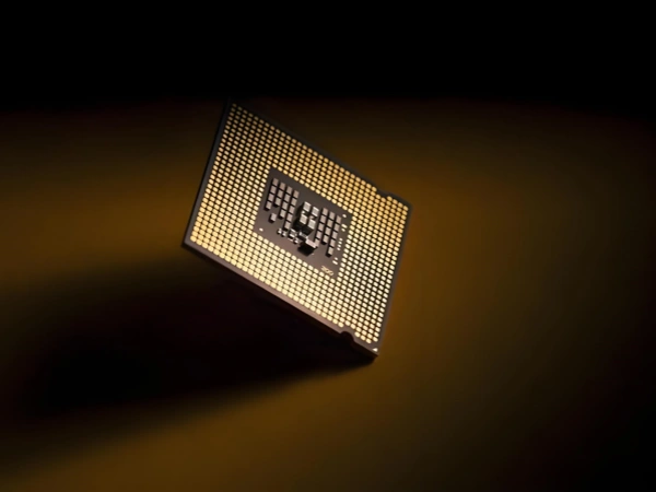
Complex interconnections. Defined build requirements.GreatPCB multilayer PCB example; construction shown for reference.
PCB manufacturing since 2002
Established manufacturing foundation
Fabrication + assembly
One coordinated project scope
Multilayer & HDI options
Construction reviewed against your files
Inspection & testing
Coverage defined for your build
Start with the right board category
What is a semiconductor PCB?
A semiconductor PCB is a printed circuit board used to support semiconductor devices, evaluation hardware, test interfaces or semiconductor equipment electronics. It provides electrical connections and mechanical support through copper conductors and an insulating substrate. The correct construction depends on the board’s function, signal requirements, power delivery and operating environment.
In chip testing, the term can describe an ATE load board, burn-in board, socket board or probe-card interface PCB. In equipment, it may describe a control, sensing or power board. These applications need different manufacturing and acceptance plans.
Application-led manufacturing
Which semiconductor board are you building?
Start with the job the board must perform. Share the application and operating conditions so the manufacturing review addresses the right electrical, mechanical and assembly risks.
01 / DEVICE VALIDATION
IC Evaluation & Development Boards
Boards for evaluating packaged devices, bringing up firmware and checking interfaces. Review package escape routing, decoupling, connector access and assembly orientation.
Specify: package footprint, supply rails, interface requirements and bring-up procedure.
02 / FINAL TEST
ATE Load & Interface Boards
Boards connecting a device under test (DUT) to automated test equipment (ATE). Review signal paths, reference planes, power distribution and socket or connector geometry.
Specify: tester interface, DUT socket drawing, impedance targets and mechanical datums.
03 / RELIABILITY HARDWARE
Burn-In & Reliability Test Boards
Hardware used to apply defined electrical and thermal stress to devices. Review laminate suitability, temperature-rated components, socket loading and current paths.
Specify: temperature, exposure duration, cycling profile and per-site current.
04 / CONTACT INTERFACE
Socket & Adapter Boards
Interconnect boards for device sockets, connectors and fixture adapters. Review pad geometry, mounting features, surface finish and contact assembly requirements.
Specify: contact design, mating cycles, alignment tolerances and assembly instructions.
05 / WAFER-TEST INTERFACE
Probe-Card Interface PCBs
The PCB portion of a wafer-test interface may require dense routing and precise mechanical alignment. Submit the construction for feasibility review; probe needles, MEMS probes and full-system calibration are separate scopes.
Specify: PCB drawings, connector layout, routing requirements and flatness limits.
06 / EQUIPMENT ELECTRONICS
Semiconductor Equipment Control Boards
Control, sensor-interface and power electronics for semiconductor manufacturing equipment. Review isolation, current capacity, connector retention and service conditions.
Specify: equipment environment, power loads, safety-related requirements and functional tests.
Application categories identify requirements for quotation. Acceptance of specialized ATE, burn-in and probe-card interface designs depends on engineering review of the submitted construction.
Requirements that change the build
Match the PCB construction to the test or equipment task
Layer count alone does not define suitability. The signal path, contact interface, temperature exposure and verification method must be considered together.
| Board category | Main manufacturing focus | Information needed |
|---|---|---|
| ATE load / interface board | Signal integrity, power paths and contact alignment | Stackup, impedance notes, socket drawings and board datums |
| Burn-in board | Thermal exposure, current capacity and socket/component ratings | Temperature-time profile, current loads and assembly material limits |
| Probe-card interface PCB | Routing density, registration and mechanical fit | Via structure, connector map, thickness and flatness requirements |
| IC evaluation board | Package routing, assembly accuracy and test access | Footprints, BOM, placement data and bring-up checks |
| Equipment control board | Power, isolation, environmental exposure and serviceability | Electrical loads, drawings, environmental limits and test procedure |
Before production release
Define the details that control manufacturability
Material & thermal exposure
Specify the laminate grade or approved equivalent, copper weight and relevant material properties. For elevated-temperature service, review thermal expansion, exposure duration and the ratings of sockets, components and solder materials together. Tg alone is not an operating-temperature rating.
Stackup & controlled impedance
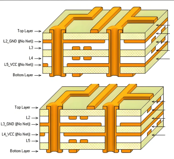
Identify signal layers, reference planes, dielectric thicknesses, impedance targets and tolerances. Include coupon and reporting requirements where needed. Low-loss materials should be selected for the actual signal path rather than every board in the equipment. Explore high-frequency PCB options and stackup planning.
HDI routing & via structures
Define microvia layer pairs, blind or buried vias, via-in-pad treatment and any sequential-lamination requirements. Package pitch and socket pin fields influence escape routing; the released construction must remain within the agreed process capability. Review our HDI PCB capability.
Contact finish & mechanical fit
Differentiate solderable pads from repeated-mating contacts. Define the required finish, plating specifications, mounting holes, datum references and flatness limits. The finish used for assembly may not be suitable for a high-cycle contact surface.
Assembly & component control
Provide approved part numbers, substitution rules, socket installation instructions and connector orientation. Define ESD handling, moisture-sensitive component controls, cleanliness requirements and any programming files in the project documentation.
Verification with a defined scope
What should a semiconductor PCB test plan cover?
Separate bare-board integrity, assembly quality and application performance. Each answers a different question and needs its own acceptance criteria.
01 / BARE BOARD
Electrical & construction checks
Define continuity and isolation testing, dimensional checks and any required impedance coupons or cross-section records. These checks verify the board against the agreed fabrication requirements. See PCB testing.
02 / ASSEMBLY
Placement & solder inspection
Choose inspection methods for the package risks: SPI, AOI, visual checks or X-ray for hidden joints where applicable. Include socket alignment and connector installation checks in the control plan. Review assembly inspection and testing.
03 / APPLICATION
Functional & interface validation
Provide a procedure, fixtures, firmware, operating limits and pass/fail criteria. Tester correlation, contact performance and application-level measurements require the appropriate equipment and agreed responsibility.
Manufacturing a burn-in board and performing IC burn-in are separate services. Bare-board electrical testing and assembly inspection also do not establish tester correlation or semiconductor device qualification. Define these deliverables explicitly before ordering.
From files to repeat builds
A controlled path from prototype to production
Carry forward approved revisions, materials, assembly instructions and test criteria so subsequent builds use a consistent manufacturing baseline.
01
Review the design package
Align Gerbers, drill data, stackup, BOM, placement files, drawings and application requirements. Resolve construction questions before quotation.
02
Approve the build scope
Agree materials, component sourcing, assembly processes, inspection coverage, functional tests and required documentation.
03
Verify the first build
Use the agreed inspection records and customer validation to assess the prototype. Capture changes in a controlled revision.
04
Release repeat production
Freeze approved build data, substitution rules and reporting requirements. Review engineering changes before the next run.
GreatPCB / PCB + PCBA
One coordinated manufacturing partner
Founded in Shenzhen in 2002, GreatPCB provides PCB fabrication and assembly services for global electronics projects. The service scope includes component sourcing, SMT and through-hole assembly, IC programming, inspection and functional testing according to project requirements.
For semiconductor-related hardware, start with a file review that connects your application to the available PCB, assembly and testing processes. Specialized constructions and qualification requirements are confirmed during engineering review.
Make the next step practical
What do we need for a semiconductor PCB quote?
Send the current design revision and identify whether you need bare boards, assembled boards or an assembly with defined functional tests. Include application-specific requirements with the files.
If the stackup or test scope is still open, mark the undecided items. Engineering review can identify the information needed to finalize feasibility and quotation.
Or contact sales@greatpcb.com.
- Fabrication dataGerbers, drill files, board outline, fabrication drawing and revision identification.
- Construction & material notesStackup, laminate, copper, via structures, finish, impedance and tolerance requirements.
- Assembly packageBOM with manufacturer part numbers, pick-and-place data, assembly drawings and approved alternates.
- Socket & equipment interfacesSocket and connector drawings, mounting datums, alignment limits and tester or fixture interface details.
- Operating & verification requirementsTemperature profile, current loads, inspection scope, functional tests, fixtures and report requirements.
- Order scopePrototype and production quantities, requested delivery date, sourcing scope and packaging requirements.
Common engineering questions
Semiconductor PCB FAQs
Clear definitions help you request the right board construction and manufacturing scope.
Is a semiconductor PCB the same as an IC substrate?
No. A board-level PCB connects components or forms a test or equipment interface. An IC package substrate connects a semiconductor die within its package and can require different materials, feature sizes and manufacturing processes. Confirm package-substrate requirements separately.
How does a load board differ from a burn-in board?
A load board connects a DUT to ATE for electrical measurements and functional tests. A burn-in board supports devices during a defined stress profile. Load-board requirements often emphasize signal paths and interfaces; burn-in hardware adds temperature exposure, component ratings and power delivery considerations.
Do all semiconductor boards need low-loss materials?
No. Material selection depends on bandwidth, routing length, thermal exposure and reliability requirements. A high-speed test interface and an equipment control board may need different laminates. Specify the actual signal and environment requirements before selecting a material.
Can GreatPCB review specialized semiconductor test boards?
Submit your stackup, fabrication data, socket drawings and test requirements for engineering review. Specialized load boards, burn-in boards and probe-card interface PCBs are evaluated against the requested construction and verification scope before acceptance.
Does PCB assembly include semiconductor device qualification?
Assembly inspection checks the built hardware against its acceptance plan. Semiconductor device qualification, tester correlation and IC burn-in require separate procedures, equipment and responsibilities. Specify these activities separately if they are part of your project.
What determines cost and lead time?
Construction complexity, materials, via processes, finish, component availability, quantities, fixtures and test scope affect the quotation. A delivery commitment follows review of the released files and sourcing requirements.