What is PCB Warping and How to Resolve It
To ensure accurate placement of SMT components, the PCB must be completely flat. The placement machine must release SMT components at the same height above the PCB for all components. [...]
To ensure accurate placement of SMT components, the PCB must be completely flat. The placement machine must release SMT components at the same height above the PCB for all components. [...]
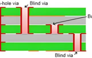
When routing needs to switch layers, vias must be added. Vias should be placed whenever ground planes are stitched, high-frequency lines are protected, or the shortest return path is established. [...]
In electronics, capacitors are crucial for ensuring the stability and reliability of PCBs. You might frequently see 0.1uF and 0.01uF capacitors used around chips as bypass and decoupling capacitors. Why [...]
In circuit design, it's common to see resistors in series with the data lines (D+ and D−) of USB interfaces on schematics. These resistors are often explained as being for [...]
The PCB half hole is widely used in the PCB manufacture of modern circuit boards, which can make the connection between electronic circuit board components close, and also enhance the [...]
In PCB design rules, there are numerous empirical formulas for designers to reference. However, is there a simpler method to address practical issues? Even if a ground copper plane has [...]
It is widely known that PCB routing should avoid right angles or acute angles. This rule is emphasized in textbooks and company technical specifications, and some even use it as [...]