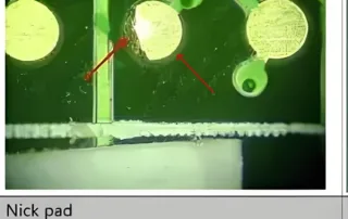
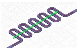
High-Precision Multi-layer PCBs, HDI, and Turnkey Assembly Services.

PCB CONSULTATION

Ten Golden Rules: Best Practices for Optimizing PCB Design

Despite the increasing integration of semiconductors and the availability of off-the-shelf systems on chips (SoCs) for many applications, as well as the growing accessibility of powerful, ready-to-use development boards, many [...]

By |2024-10-21T16:59:25+08:002024-10-21|PCB Design, PCB layout|0 Comments

Understanding ICD Issues in PCB Manufacturing: Causes and Solutions

In the vast realm of the electronics manufacturing industry, PCBs (Printed Circuit Boards) are undoubtedly the shining stars. They are not only indispensable components in electronic devices but also serve [...]

By |2024-10-07T13:56:12+08:002024-10-07|FCB FAB, PCB Design|0 Comments

The Role and Considerations of Serpentine Traces in PCB Design

Any trace on a PCB that carries high-frequency signals can cause signal delay. The main purpose of serpentine traces is to compensate for parts of a group of related signals [...]

By |2024-09-24T16:03:38+08:002024-09-24|HDI PCB, PCB Design, PCB layout|0 Comments

Why Your PCB Fails Despite Using the Manufacturer’s Schematic

You've followed the schematic provided by the chip manufacturer, but your PCB still has issues. It may be unstable, not hitting performance targets, or failing EMC tests. Is it human [...]

By |2024-09-14T17:44:50+08:002024-09-14|PCB Design, PCB layout|0 Comments

PCB Design in the 5G World: Challenges and Solutions

PCB Design Requirements for 5G Applications In 5G applications, the key PCB design requirements include high-frequency, high-speed materials, high-density interconnects (HDI), impedance matching, layer stack-up planning, signal integrity for trace [...]

By |2024-09-10T15:09:03+08:002024-09-10|HDI PCB, PCB Design|0 Comments
Go to Top