What is PCB Warping and How to Resolve It

To ensure accurate placement of SMT components, the PCB must be completely flat. The placement machine must release SMT components at the same height above the PCB for all components.
If the PCB is warped or uneven, the machine will not be able to maintain a constant height while placing components on the board, affecting placement accuracy, especially for fine-pitch components.
Additionally, a flat PCB helps keep SMT components in place during reflow. If high temperatures in the reflow oven cause the PCB’s flatness to change, SMT components may shift due to floating in the molten solder, leading to solder bridging and open circuits.
1. What is PCB Warping?
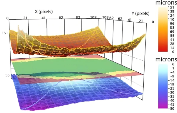
PCBs are typically made from fiberglass and other composite materials, and most PCBs are single-layered and quite simple. PCB warping refers to the change in the shape of the PCB, as shown in the image below, which illustrates clear PCB warping.
Insert image description here
2. What is the Standard for PCB Warping?
According to IPS standards, the warpage (WD) of a PCB intended for SMT placement should be less than or equal to 0.75%. In other words, if WD exceeds 0.75%, it should be considered warped or defective.
In practice, for PCBs that only need to be plugged in without components, the flatness requirement is lower, and the WD standard can be less than or equal to 1.5%.
Of course, to meet higher customer demands, Greatpcb can pursue stricter standards, with some WD standards requiring less than or equal to 0.5%, or even less than or equal to 0.3%.
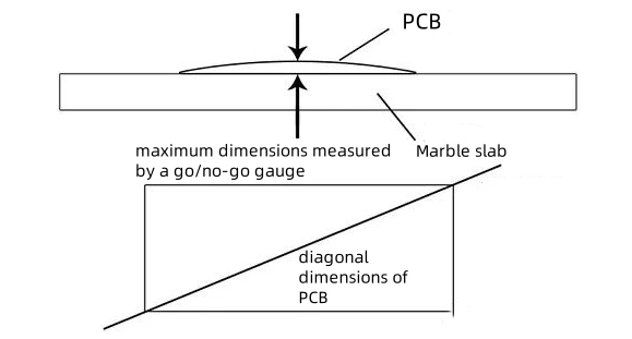
3. PCB Warping Calculation Formula
Warping, as the term suggests, refers to whether the PCB is flat and whether it can perfectly fit into the board’s holes and surface mount pads.
Warping typically refers to the deformation of the surface of a plastic part that does not conform to the designed shape. There are many factors affecting warping, so attention must be paid during production. After all, even a minor error could result in the entire circuit board being scrapped. So, how is PCB warping calculated?
PCB warping calculation formula:
Warping = Single-angle warping height / (PCB diagonal length * 2) * 100%
Insert image description here
In automatic insertion, if the PCB is not flat, it can cause misalignment and even lead to the automatic insertion machine getting stuck. If the board bends after component soldering, it becomes very difficult to neatly cut component leads, eventually resulting in the PCB not fitting into sockets in the chassis or machine, effectively scrapping the circuit board. For manufacturers, encountering PCB warping is particularly distressing, mainly due to the financial loss.
4. Causes of PCB Warping
Causes of PCB Warping
The weight of the circuit board itself can cause deformation and warping.
Generally, the reflow oven moves the PCB forward using chains, supporting the entire board from both sides. If the board has heavy objects or is too large, due to the board’s weight, it may sag in the middle, causing the board to bend.
Excessive V-cut depth can cause warping at the V-cut areas.
V-Cut is a major cause of structural damage to the board, as V-Cut creates slots in the original large sheet, making it prone to warping. The impact of materials, structures, and patterns on board warping: PCBs are pressed from core boards, prepreg, and outer copper foils. When core boards and copper foils are pressed together, they can deform due to heat. The amount of warping depends on the thermal expansion coefficients (CTE) of the two materials.
- The CTE of copper foil is approximately 17×10^-6.
- For standard FR-4 substrate, the Z-direction CTE at Tg point is (50-70)×10^-6; above Tg point, it is (250-350)×10^-6. Due to the presence of glass cloth, the X-direction CTE is generally close to that of copper foil.
Warping Caused During PCB Processing
The causes of PCB processing warping are complex and can be divided into thermal stress and mechanical stress. Thermal stress mainly arises during the pressing process, while mechanical stress occurs during board stacking, handling, and baking.
Warping caused during copper-clad board processing.
Copper-clad boards are double-sided and symmetrical in structure, with no patterns. The CTE of copper foil and glass cloth are almost the same, so warping due to different CTEs during pressing is minimal. However, due to the large size of the copper-clad board press, temperature differences across the heating plates can cause variations in resin curing speed and degree across different areas. Additionally, different heating rates can result in significant differences in dynamic viscosity, creating localized stress. This stress generally balances after pressing but may gradually release and deform during subsequent processing.
Warping caused during PCB pressing.
The PCB pressing process is a major source of thermal stress. Similar to copper-clad board pressing, it generates localized stress due to variations in curing processes. With thicker boards, more varied pattern distributions, and more prepreg, thermal stress is more difficult to eliminate compared to copper-clad boards. The stress in the PCB board releases during subsequent drilling, shaping, or baking processes, leading to board deformation.
Warping caused during solder mask and silkscreen curing.
During curing, solder mask inks cannot stack on each other, so the PCB board is placed on racks for curing. The solder mask temperature is around 150℃, exceeding the Tg of the copper-clad board, making the PCB prone to softening and unable to withstand high temperatures. Manufacturers must evenly heat both sides of the substrate and keep processing time as short as possible to reduce board warping.
Insert image description here
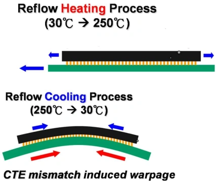
Warping caused during PCB cooling and heating.
The solder oven temperature ranges from 225℃ to 265℃, and the hot air solder leveling time is 3-6 seconds. The hot air temperature ranges from 280℃ to 300℃. After solder leveling, the board is placed in the solder oven from room temperature and treated with room-temperature washing within two minutes after removal. The entire hot air solder leveling process involves sudden heating and cooling. Due to differences in board materials and uneven structures, thermal stress inevitably causes microscopic strain and overall warping areas.
Insert image description here
Warping caused by improper storage.
During semi-finished product storage, PCBs are generally placed firmly on racks. If the rack’s tension is not properly adjusted or if the boards are stacked during storage, mechanical deformation can occur. This issue is more severe for thin boards under 2.0mm.
Engineering Design Reasons
- Uneven copper area on the board, with more on one side and less on the other. In areas with sparse lines, surface tension is weaker compared to dense areas, and high temperatures can cause board warping.
- Due to special dielectric or impedance relationships, the laminate structure may be asymmetric, leading to board warping.
- Excessively large and numerous cutouts in the board can cause warping at high temperatures.
- Excessive number of panels on the board, with hollow spaces between panels, especially with rectangular boards, can also lead to warping.

5. How to Improve PCB Warping?
1. Considerations During PCB Design
Copper Pour on the Board to Increase Surface Tension
When the board length exceeds 80 mm and there is no copper, and the board thickness is less than 1.0 mm, warping can occur. If the board cannot be pressed or thickened, use heavy pressing to correct warping.
Copper Plating in Hollow Areas and Process
When there are many hollow areas or the board is too large, it is prone to warping after reflow soldering. During PCB manufacturing, dielectric layers are evenly distributed, but uneven copper layer distribution causes warping. Designers must balance copper patterns and circuit areas on each layer of the board, as well as component layout, assembly distribution, and thermal distribution to minimize warping.
For example, if the top surface has a large copper area and the bottom surface has minimal copper traces, the PCB will tend to warp more after etching. Designers should ensure that the copper pattern area on both outer layers matches as closely as possible. If there is a significant copper area difference, adding a separate copper grid on the thinner side can help balance the two.
Recommendations: Plate copper in hollow areas to reduce warping; also, plate copper inside the board if it does not affect functionality; lastly, apply copper plating along the edges during the process.
Use the Same Brand for Core and PP Sheets
The core and PP sheets of multi-layer boards must be from the same brand to avoid warping. For example, if a 6-layer board has asymmetric PP sheets (thinner in the 2-3 core layers and thicker in the 4-5 core layers), pressing can cause warping. Therefore, core and PP sheets should be from the same brand to ensure consistent thickness and symmetry.
Maintain Symmetry in Prepreg Layer Arrangement
Manufacturers must ensure that the arrangement of prepreg layers remains symmetrical. For example, in a six-layer board, the thickness between layers 1-2 and 5-6 should ideally be the same, including the number of prepreg sheets. This prevents warping after lamination.

2. Considerations During PCB Processing
Pre-Cutting PCB
Bake the copper-clad board before cutting (150°C for 8±2 hours) to remove moisture and fully cure the resin, which helps eliminate residual stress in the PCB and prevents warping. Many double-sided and multi-layer boards still adhere to baking steps before or after cutting, though some factories have exceptions. The drying time varies among PCB manufacturers, ranging from 4 to 10 hours. It is recommended to determine based on board grade and warp requirements.
Baking the entire board before cutting or cutting and then baking are both feasible methods. It is advisable to bake after cutting, and inner boards should also be baked.
Prepreg Orientation
Prepregs shrink differently in the warp and fill directions. Proper differentiation during cutting and lamination is crucial to avoid warping after lamination. If prepregs are not differentiated in warp and fill directions, warping can occur even with pressure applied to the baked board.
To distinguish between warp and fill directions: For prepreg, the rolling direction is warp, and the width direction is fill; for copper foil, the long side is fill, and the short side is warp. Consult manufacturers or suppliers if uncertain.
Stress Relief After Lamination
After thermal and cold pressing, remove burrs from the multi-layer board and lay it flat in an oven at 150°C for 4 hours to gradually release internal stress and fully cure the resin. This step is essential and should not be omitted.
Straightening Thin Boards During Plating
For ultra-thin multi-layer boards (0.4-0.6mm), use specialized clamping rollers during surface and pattern plating. Clamp the thin board onto the rollers and use cylindrical rods to hold it in place. This prevents deformation after plating.
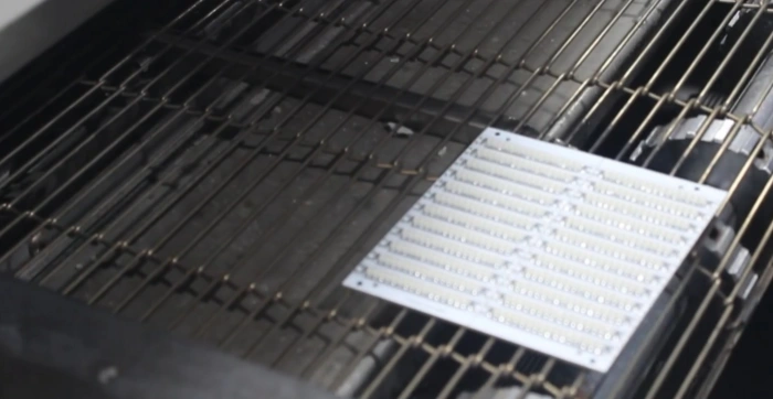
Cooling Boards After Hot Air Leveling
During hot air leveling, the PCB is affected by high temperatures (approximately 250°C). After removal, place it on a flat marble or steel plate to cool naturally before sending it to post-processing machines for cleaning. This helps prevent warping.
Some factories immediately place boards into cold water after hot air leveling to enhance solder surface brightness. This thermal shock can cause warping, delamination, or bubbling. Installing an air-cushion bed for cooling on equipment is also an option.
6. PCB Warping Repair Methods
Warping Repair During PCB Processing
Boards with significant warping can be corrected using a roller leveling machine before proceeding to the next process. Many PCB manufacturers find this method effective for reducing final PCB warping.
Repairing Warped Finished PCBs
For finished boards with significant warping, roller leveling machines may not be effective. Some PCB factories use small pressure machines (or similar fixtures) to press the warped PCB, applying pressure for several hours to ten hours for cold pressing. The effectiveness varies; the results may not be significant, and the board may rebound.
Some PCB factories heat the small press to a certain temperature before performing hot pressing, which can improve results compared to cold pressing. However, excessive pressure can deform the traces, and high temperatures may cause defects like discoloration of solder flux. Both cold and hot pressing require several hours to see results, and rebounding after pressing is common.
Recommended is the use of bow-shaped molds for hot stamping leveling. Depending on the PCB area, use simple bow molds. Two types of leveling operations are proposed:
Baking and Leveling Using Bow Molds
Place the warped PCB with the curved side against the mold’s curved surface, adjust the fixture screws to counteract the warping, and bake the mold in an oven at a certain temperature. Under heat, the board’s stress will relax, and the deformed PCB will return to a flat state. However, avoid excessive temperatures to prevent resin discoloration or substrate yellowing. Lower temperatures may require longer to fully relax stress.
Generally, use the glass transition temperature of the substrate as a reference temperature for baking. This is the temperature at which polymer chains can rearrange and stress is fully relaxed.
The bow mold method is effective and cost-efficient. Ovens are commonly available in PCB factories, and the leveling operation is straightforward. For multiple warped boards, several bow molds can be used simultaneously, with shorter drying times (around minutes), enhancing efficiency.
Softening and Leveling Using Bow Molds
For boards with minor warping, place the PCB in a preheated oven (temperature set according to the substrate’s glass transition temperature) and bake until softened. Adjust pressure screws on the bow mold to counteract warping, then allow the board to cool and set. This method is effective for reducing warping, even after wave soldering, and has minimal impact on board appearance.
PCB warping is a challenging issue for manufacturers, impacting yield and delivery times. Using bow-shaped molds for hot stamping leveling, with appropriate process adjustments, can effectively address warping and meet delivery deadlines.
This concludes a simple introduction to PCB warping, its causes, and solutions.
Table of Contents

Related Posts
PCBA Prototype
July 21, 2026
PCBA Prototype
July 17, 2026