Do You Really Know All About PCB Via Holes?

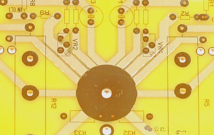
When routing needs to switch layers, vias must be added. Vias should be placed whenever ground planes are stitched, high-frequency lines are protected, or the shortest return path is established. In BGA package routing, the absence of vias can make routing almost impossible. While not every PCB is so complex in terms of via design, even a standard PCB contains a significant number of vias. The placement of vias may seem random, but there is a lot of science behind it, especially in high-speed circuits where the distribution parameters of vias must not be overlooked. The placement and connection of vias must be carefully considered, and in some cases, calculations and simulations are required to determine the type and size of the via.
Vias and Bypass Capacitors
For example, the position of vias affects the actual effectiveness of bypass capacitors. In the case of capacitor placement, the first example (C1) has a trace that is too narrow, leading to high inductance. The second example (C2) has a long trace, resulting in significant distribution parameters. The third example (C3) is acceptable, while the fourth example (C4) reduces impedance further by using two vias, allowing the capacitor to be placed on the bottom layer to save space on the top layer for routing.

Proper Via Placement
It’s important to note that vias should not be placed between the capacitor and the IC power pin, as this would increase the parasitic parameters between the bypass capacitor and the power pin.

Advanced Via-in-Pad Techniques
A more advanced approach is to place the via directly on the pad, as shown in the image below. In the past, placing a via on the pad was discouraged because it couldn’t be protected with solder mask, leading to issues such as solder leakage and voids during the soldering process. However, with the advancement of PCB manufacturing technology, Greatpcb has mastered the via-in-pad process, resolving these issues.


Preventing Solder Leakage
To prevent solder leakage, vias are first filled with resin or copper paste and then covered with a layer of copper plating on the pad. This solution not only eliminates solder leakage but also ensures that the appearance and performance are indistinguishable from standard pads.
Application of Via-in-Pad
This via-in-pad technique is especially useful for dense circuit boards where routing space is limited.

For instance, with a 0.4mm pitch BGA package, via-in-pad is almost the only option.

Types of Vias:
- Through-Hole Via: A common via that runs through the entire PCB, connecting the top and bottom layers. This type is the easiest to implement and has the lowest cost.
- Blind Via: Located on the top or bottom layer of the PCB, connecting to internal layers without passing through the entire board.
- Buried Via: Situated within the inner layers of the PCB, connecting multiple layers without extending to the outer surfaces.
- Micro Via: A via with a diameter of less than 0.25mm, primarily used in high-density interconnect (HDI) designs, created using laser drilling or plasma chemical etching techniques.
- Via-in-Pad: A via directly placed on a pad, used when routing space is extremely tight or when high-density routing is required.

Via Protection:
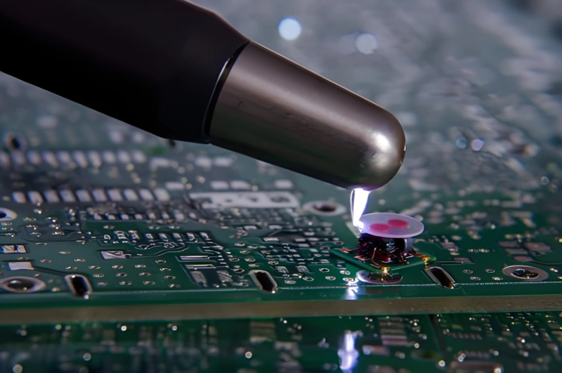
After vias are created, they are typically covered with solder mask or filled with resin and copper paste to prevent solder leakage, voids, and short circuits. In high-speed boards, these measures are also crucial for maintaining stable and controlled distribution parameters. During automated production, vacuum pick-and-place machines may require vias to be covered to prevent air leakage.


Process Parameter Requirements:
Generally, via diameters range from 0.15mm to 0.5mm. Smaller diameters increase manufacturing difficulty, so it’s preferable to keep via diameters above 0.2mm. However, larger vias aren’t always better. If the via diameter exceeds 0.5mm, the solder mask may not be able to cover it properly. Ideally, the pad’s outer diameter should be 0.15mm larger than the via hole.
Table of Contents
Related Posts
PCBA Prototype
April 27, 2026


