SMT Moves Inside Advanced Packages
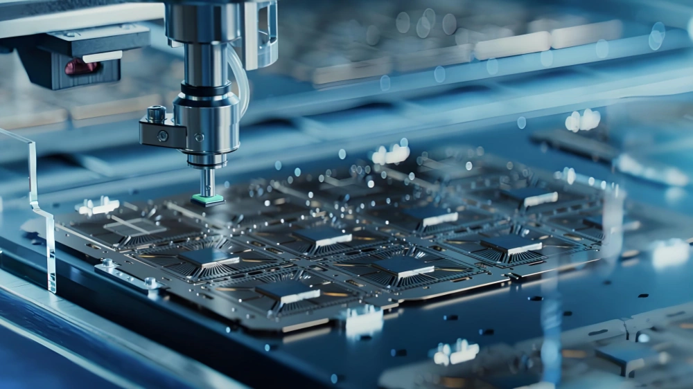
SMT is no longer just for assembling packaged chips onto PCBs. It now moves inside advanced semiconductor packages — bringing new challenges in materials, inspection, and testing that blur the lines between PCB and IC manufacturing.
Surface mount technology (SMT) has grown far beyond its use as a way to assemble packaged chips onto printed circuit boards with no through-holes. It is now moving inside packages that will themselves be mounted on PCBs.
But the SMT for advanced packaging is not the same as the SMT we are used to.
"Many systems contain multiple ASICs, a lot of memory, and all of these are integrated in a very small space," said Kenneth Larsen, product marketing director at Synopsys. "It is almost like you have compressed a whole PCB into a very small form factor."
Advanced packaging uses interposers or other substrates to hold the chips. These interposers are like mini PCBs, even though they are made from different materials. But the dimensions of metallization redistribution layers (RDL) are usually much larger than those used on PCBs, even though they are large by semiconductor standards. So, ideas must be brought in from both the PCB side and the semiconductor side to make sure of good manufacturability.
"Some companies are more PCB-centric, starting from the packaging PCB side. But there are other companies that are more chip-centric, looking at it from the chip side," said Marc Swinnen, product marketing director for semiconductors at Ansys. "But these two worlds are moving closer together, and many companies are not ready for it."
This puts chipmakers in a difficult spot. "Are you going to use the modern tools of the semiconductor fab?" asked Steve Ledford, general manager of device interfaces at Teradyne. "Or are you going to use the modern tools of the PCB and SMT manufacturing people?"
Although advanced packaging is not new, it is still early in its production life, and its use tends to be limited. As costs come down and more applications use the tighter integration this packaging offers, more companies will be able to take advantage of it. So, it may help to step back to a higher level and get some perspective between the original SMT and the newer variants.
"In between the stacking phenomenon and SMT, advanced packaging sits between traditional front-end and traditional back-end," said Subodh Kulkarni, president and CEO of CyberOptics. "That is where all the innovation is happening now. Open any modern device, and the advanced packaging strung together looks very different from a circuit board of 10 years ago."
An in-package interposer does the same job as a PCB. It helps connections between the components mounted on it. Also, it provides the routing that will finally connect to bumps and the PCB. Many ideas needed for PCB manufacturing come into play on the interposer, just in miniature. Whole systems with computing, memory, and even analog I/O can be assembled and then mounted on a PCB as one package.
This sounds like shrinking a PCB down to fit onto a meta-PCB, but it is not that easy. Any such assembly process needs inspection and test to make sure of quality. But tools for inspecting and testing PCBs do not always work at the package level. It is all SMT, but different equipment is needed depending on the materials used and the feature sizes on the interposer.
Materials for Substrates
High-volume commercial PCBs are often made from FR-4, a fiberglass/epoxy mix that has been a favorite for PCBs for many decades. While it can be shrunk down for small mezzanine cards and other tiny boards, the minimum line spacing is in mils, not microns. The minimum pitch is usually in the range of 5 or 6 mils (a bit lower for special applications), which means over 100 microns.
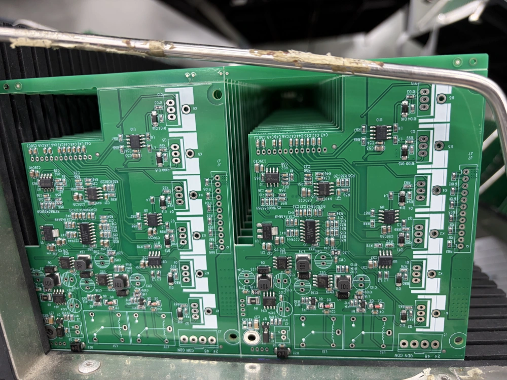
Converting to microns is useful, because advanced packaging substrates can support dimensions in microns. So right away there is an immediate shrink by an order of magnitude. Their exact position in the micron world also depends on the substrate material.
Two words seem to be used when describing things that look like "mini PCBs" inside a package. Sometimes they are simply called substrates, and sometimes they are called interposers. There seems to be no formal definition that separates a substrate from an interposer, but common usage in this context seems to apply substrate to organic materials and interposer to inorganic materials. (Technically, an interposer is a substrate.)
A PCB may have many layers for complex routing and shielding, but substrates and interposers tend to have very few layers — perhaps only one, often called a redistribution layer (RDL). Organic substrates are often used in so-called panel applications. These are similar to semiconductors in that multiple units are fabricated on one large piece before being cut into individual units. The big difference is that, because of the way they are made, panels can be rectangular. This means nothing is wasted when cutting them apart. This technology mainly comes from the display industry.
"Why square chips work on round wafers is not because wafers are the ideal choice for square objects," said Ledford. "It is because that is how silicon ingots are pulled."
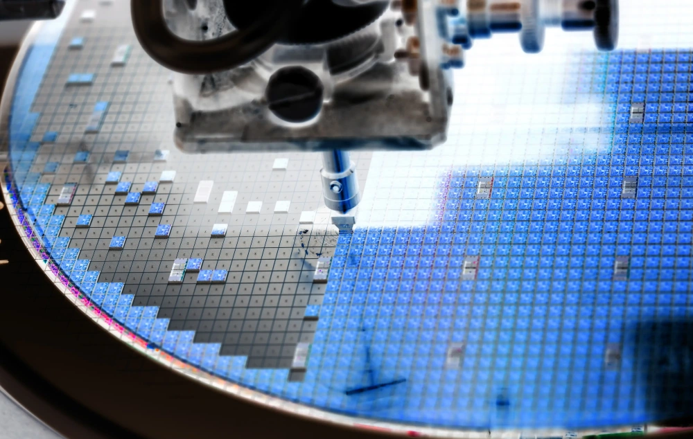
Glass is another promising candidate that is still in the early stages of development. "Glass can be either round or square," noted Ledford. Glass substrates are also often called interposers.
So these are the three basic variants of SMT substrates: PCB, panel, and interposer. They have notable cost and size differences.
Dimensions and Manufacturing
"Everything is moving toward semiconductor-like dimensions," said Ledford. "It is only a matter of time. When I just graduated, mainstream semiconductors had 1-micron line widths. If you look at where advanced packaging is now, it is already very close to 1-micron lines and spaces. It took only 30 years to get to this point."
There are two key aspects to the dimensions needed for any of these materials. First, there is the minimum pitch. But just as important is the control over those dimensions.
"Testing and measurement are all about 50 Ω controlled impedance," said Ledford. "That means the maker of that line needs to control dimensions down to a quarter of a micron. Well, if I go and talk to any of my PCB shops, none of them come close to that level of dimension control."
The main reason is chemistry. PCBs are made using wet chemistry, which limits dimensions and tolerances. "The wet chemical processes that dominate PCB and [traditional] SMT do not have the dimension control you need," said Ledford. "What kind of process lets you control quarter-micron lines and spaces? Dry processes — sputtering, dry etching, and so on — come mainly from the semiconductor world."
While several PCBs can be processed together in some kind of bath, panels and wafers must be handled one by one in their reaction chambers. This is one of the main costs linked to the smaller form factors.
"Semiconductor manufacturers are moving to panel-level packaging mainly because of the large chips in system-in-package (SiP)," said Woo Young Han, product marketing manager at Onto Innovation. "Multiple chips, including CPU, GPU, DSP, and memory, are packaged into one single base, and the result is much larger than the traditional chip sizes used in the semiconductor industry. SiP chip sizes can be as big as 100 mm. So, a 600 mm rectangular panel is better than a 300 mm round wafer when making large SiP chips."
Silicon interposers are limited by wafer size, so they are more useful for integrating processors with more limited memory. Chiplets are also candidates for integration into these smaller packages.
Using panels can give larger chips, but at the cost of how close you can put the lines or chips together. "Panel-level packaging may have a bigger GPU or CPU, but not necessarily very close to the chiplets," said Robert Cid, product line manager for white light interferometers at Bruker.
That said, while one might hope panels would be a middle ground for wafer-level integration, it may actually go the other way. "For companies that want to do more integration, I think panel-level packaging is becoming more and more of a doable solution," noted Cid. "If wafer-level packaging starts moving to bigger substrates, packaging costs could drop even more."
The main functional difference between a PCB and any of these other options is the number of interconnects that can be managed. "You are not talking about a few 40-micron I/O pads," said Ledford. "You are talking about thousands of 40-µm I/O pads."
Others agree. "You can have thousands of these microbumps and very dense traces," noted Randy Fish, director of silicon lifecycle management marketing in Synopsys' digital design group. "And being able to have redundant interconnects is an essential part of this."
Inspection
One of the main process differences between PCBs and advanced packaging lies in inspection — especially the ability to rework where defects are found.
"In a typical PCB inspection flow, an inspection module checks the PCB, and then the PCB is moved to a review station for operator review — and then sent to a repair station to fix found defects," explained Han. "In the semiconductor wafer inspection world, fixing single defects is unthinkable in both front-end and back-end semiconductor processes."
Humans are still present in PCB inspection. "Because of the historical nature of the PCB industry, they still see a lot of manual inspection stations with operators looking through microscopes," said Ledford.
Kulkarni from CyberOptics described his surprise when he saw the end of a DIMM production line. "There were 20 people standing around that area with bright white lights," he said. "They were physically picking up each memory board from a conveyor belt and visually inspecting both sides before dropping them into plastic bags."
The DIMMs went through a final I/O test, but they were hot when plugged in. Half a minute later, when taken out, they had clearly cooled down, and they did not pull out as easily — sometimes disturbing the memory on the board. "Even though the I/O check looked good, it was not good when the customer got it," Kulkarni explained.
Adding an automated final inspection step now allows intervention for any board that needs rework, without human inspection.
Sockets for holding large CPUs or other such expensive chips are another example. Sockets are used so that if a board goes bad, the high-value chip can be easily removed and moved to a new board, instead of being thrown away with the board.
"In a 3 × 3 inch square, you have 10,000 pins," said Kulkarni. "And these are actually little fuzzy copper things that come out and bend, because there has to be some kind of spring."
This makes it very hard for a human to inspect them. Vision tools can again automate this process, improving results and throughput. So, PCB inspection is already moving toward higher levels of automation.
But moving inside advanced packaging, the size and number of signals make manual inspection completely impractical. Automation is needed. But the way these tools work is different between PCB and panel-level and wafer-level assemblies.
"Large chip sizes are common in the PCB world, and traditional PCB inspection tools use a CAD design-rule-based method," said Han. "In the semiconductor world, inspection tools are designed to find much smaller defects on highly repeating chip patterns. So, inspection tools in the semiconductor world use a golden die or adjacent die comparison method. SiP die-to-die differences are much larger compared to semiconductor wafers, and the CAD design-rule method works better than the golden/adjacent die comparison method. That is an advantage for traditional PCB inspection tools. SiP design rules are also much smaller than traditional PCB die designs — trace widths as small as 2 microns — and need sub-micron defect detection. But PCBs use trace widths larger than 10 µm, and traditional PCB inspection tools do not have the optical resolution to do sub-micron defect detection. That is an advantage for semiconductor wafer inspection tools."
Panel sizes are a bit bigger than interposer sizes, but it is still possible to use semiconductor equipment — with relaxed numbers. "If you have a 600 x 600 mm size, you need to make sure that the features across the whole panel are within spec," said Cid. "That can be a challenge. We have seen customers look for ways to speed up metrology to survey larger areas so they can assess the quality of that panel before it goes into production."
Even so, it would be wrong to assume panels and interposers have similar inspection. "We see very different requirements for wafer-level and panel-level packaging," said Cid. "We have tools designed just for panel-level packaging, with different requirements than the tools we designed for wafer-level packaging."
That said, part of this is a case where panels lag behind interposers. "The roadmap discussions we hear suggest that panel-level processing requirements will become more complex, needing some of the strict metrology you see for wafer-level packaging a few years from now," said Cid.
So, while automation and AI are entering PCB inspection, these technologies are absolutely essential for advanced packaging.
Testing Boards, Substrates, and Interposers
Testing brings together completely different mindsets. In the past, PCBs were tested using bed-of-nails testers that quickly check all the connections on a board. But each board needs a custom fixture, which adds friction to the test development process.
JTAG made this a bit easier, giving a way to link all the components on a board together and test their connectivity. This was the original goal of JTAG, before internal chip test abilities were added later. So, in principle, connections and functionality can be tested using a single JTAG port.
In contrast, ICs use internal self-test together with externally provided vectors. These vectors may use dedicated test pins or other pins that double as test access pins in test mode. One key difference from PCB test is that with ICs, functionality is tested. For PCBs, it is mostly about testing connections. The assumption is that the ICs on the PCB work based on the individual tests they went through as part of their manufacturing flow.
Advanced packaging sits between the two, and exactly when testing is done will have a huge impact on cost. That is because people are taking dies that have been tested and then separated, and placing them on a substrate or interposer that itself must be tested to make sure the connections work.
But were those dies damaged during the separation process? Does the substrate/interposer assembly need to be tested by itself, including connectivity and functionality, to make sure everything survived assembly? Should the interposer be tested before the chips are applied, and then tested again afterward? If the whole thing is to be tested, should it be tested before or after packaging — or both?
Part of the challenge is the number of internal connections that never connect to the outside. "A lot of these internal dies are not meant to talk to the outside world," noted Fish. "All the connections are die-to-die."
There are no solid answers to these questions. It will vary by application and the economics that come with it — not to mention the risk of failure. Safety-critical parts need much more testing than parts where the result of a failure is limited to annoyance or loss of goodwill for the manufacturer.
"In some cases, if the choice is there, people do want the ability to test the chips inside a complex package," said Fish. "But for low-priced or mid-range products, I do not think you can test every chip again."
There is also an important practical effect if the dies themselves are tested. "If you buy known good die, does the supplier give you their test sequence so you can run it yourself?" asked Fish.
As for the actual testing, even if the assembly looks like a mini PCB, the bed-of-nails approach is completely impractical due to the size. The pogo pins used in such fixtures are way too big. Also, a custom fixture for every chip adds an unreasonable burden and cost to the process.
JTAG can be used here as well, though it has limited signal speed. USB and PCIe are also options for dedicated test access ports that can speed up the testing of single chips and advanced packaging assemblies. In fact, this can be used for PCBs too.
"We are moving toward high-speed dedicated I/O for test," said Fish. "You plug our IP into your chip, which connects to those I/Os on the controller side, and then to the test infrastructure on the chip."
Conclusion
To sum up, surface-mount devices inside advanced packages must be made, inspected, and tested using techniques that come mostly from the semiconductor world. While many ideas may have started with PCBs, it is often not practical to shrink PCB methods down far enough.
Since packaging is a natural part of the semiconductor manufacturing process, it is no surprise that advanced packaging carries most of the semiconductor legacy. But the basic idea of attaching components to a substrate surface goes back to the PCB world. When scaled down to near-semiconductor sizes, it looks very different.