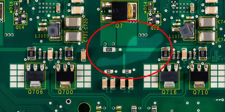
HDI PCB vs. Standard PCB: Key Differences
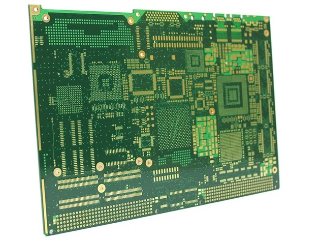
An HDI PCB is not automatically better than a standard PCB. It is a different construction approach used when conventional routing, via structures, and board dimensions no longer provide enough design margin.
The practical choice depends on the component package, escape-routing requirement, board area, layer stack-up, electrical performance, reliability target, production volume, and total cost. A conventional multilayer PCB may be the better engineering decision when the design has enough area and can be routed with through-hole vias. An HDI PCB becomes more attractive when fine-pitch components, compact packaging, or dense interconnects make conventional construction inefficient or impractical.
Quick Answer: What Is the Difference Between HDI PCB and Standard PCB?
An HDI PCB uses high-density interconnect techniques such as microvias, blind vias, buried vias, fine-line routing, and sequential lamination to fit more connections into a smaller area. A standard PCB generally relies more heavily on through-hole vias and conventional multilayer fabrication.
The distinction is not simply the number of layers. A standard PCB can be a two-layer, four-layer, or high-layer-count board, while an HDI PCB can use different structural types depending on the required interconnect density. The defining issue is how the board creates and routes electrical connections within the available space.
| Design factor | HDI PCB | Standard PCB |
|---|---|---|
| Primary interconnect technology | Microvias, blind vias, buried vias, fine-line routing | Mostly through-hole vias and conventional traces |
| Routing density | Higher | Moderate to high, depending on layer count |
| Component escape routing | Better suited to fine-pitch BGAs and compact packages | More limited when pad pitch and board area are constrained |
| Board size | Can reduce area or support more functions in the same area | Often requires more area or additional layers for equivalent connectivity |
| Fabrication | Usually involves sequential lamination and laser drilling | Often uses a simpler multilayer process |
| Cost structure | Higher process and tooling complexity | Usually simpler to fabricate |
| Design and inspection | Requires tighter registration, via, and process controls | Generally easier to design, inspect, and rework |
| Best use case | Compact, dense, fine-pitch, or highly integrated products | Cost-sensitive designs with adequate routing space |
GreatPCB’s existing overview of how HDI PCB differs from traditional PCBs provides a useful introduction. The more important engineering question is whether the additional HDI process steps solve a real design constraint.
GreatPCB supports both HDI and standard PCB manufacturing for global customers. Visit our website for more information.
What Is an HDI PCB?
HDI means High-Density Interconnect. An HDI PCB is designed and manufactured to provide more interconnections per unit area than a conventional PCB.
Typical HDI features include:
- Laser-drilled microvias
- Blind vias that connect an outer layer to one or more internal layers
- Buried vias located only within internal layers
- Fine trace and spacing rules
- Via-in-pad structures where appropriate
- Sequentially laminated build-up layers
- Shorter connections between component pads and routing layers
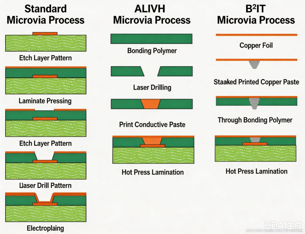
A microvia is a small-diameter via formed between adjacent layers, usually by laser drilling. Because it does not pass through the entire board, it consumes less routing space than a conventional through-hole via.
Blind and buried vias are related but not identical. A blind via connects an outer layer to an internal layer. A buried via connects internal layers without reaching an outer surface. The correct structure depends on the stack-up, component escape pattern, aspect ratio, and fabrication method. See GreatPCB’s reference on blind and buried vias in HDI PCB construction.
HDI technology is often selected when a designer must escape a dense package, reduce board dimensions, shorten critical connections, or avoid adding several conventional layers.
What Is a Standard PCB?
“Standard PCB” is a practical industry term, not one fixed construction. It usually refers to a conventional rigid PCB manufactured with mechanical drilling, plated through-holes, and standard multilayer lamination.
A standard PCB may include:
- Single-sided or double-sided construction
- Conventional through-hole vias
- Multilayer stack-ups
- FR-4 or other laminate systems
- Solder mask and surface finish
- Controlled impedance routing
- Buried or blind vias in some designs
This matters because HDI and standard PCB are not always opposites. A conventional multilayer board may already use advanced materials, controlled impedance, or selected blind vias without being classified as a full HDI design.
For a broader explanation of multilayer construction, see GreatPCB’s guide to multilayer PCB manufacturing and applications.
HDI PCB vs. Standard PCB: The Main Engineering Differences
1. Via Technology and Routing Density
The most visible difference is the way each board uses vias.
A through-hole via is mechanically drilled through the full board thickness and plated along the hole wall. It provides a robust connection, but the drill clearance and annular ring occupy routing space on every layer the via passes through.
A microvia connects only a limited number of layers. This allows traces to route more closely around dense component pads and reduces the amount of unused area consumed by via anti-pads and clearances.
HDI is useful when:
- A fine-pitch BGA cannot be escaped with through-hole vias
- Component placement leaves little routing space
- The board must become smaller without losing functionality
- Additional conventional layers would create excessive thickness or cost
- Shorter via transitions improve a high-speed interconnect design
However, a smaller via does not automatically produce a better electrical result. The design still requires appropriate reference planes, return paths, stack-up control, and impedance calculations. GreatPCB’s guidance on PCB stack-up design is relevant because HDI performance depends on the relationship between copper layers, dielectric thickness, and routing geometry.
2. Layer Structure and Sequential Lamination
A conventional multilayer PCB may be laminated in a relatively simple core-and-prepreg structure, followed by mechanical drilling and plating.
HDI fabrication commonly adds build-up cycles. A manufacturer may laminate additional dielectric and copper layers, form microvias, plate or fill them, and repeat the process. This is known as sequential lamination.
The exact structure can vary:
- 1+N+1
- 2+N+2
- Any-layer HDI
- Stacked microvia construction
- Staggered microvia construction
These labels describe the relationship between build-up layers and the central core. They should not be treated as universal quality grades. The right structure depends on the package escape pattern, layer count, board thickness, via design, and manufacturing capability.
Sequential lamination introduces additional registration, material, plating, drilling, and inspection requirements. That complexity is one of the main reasons HDI PCB cost is higher than a comparable conventional board.
3. Signal Integrity and Electrical Performance
HDI can improve electrical performance, but the benefit is design-dependent.
Shorter vias and shorter component-to-plane connections can reduce parasitic effects and via stubs. A more controlled stack-up can also help maintain reference-plane continuity and impedance targets.
These benefits are valuable for:
- High-speed digital interfaces
- RF and wireless modules
- Compact processors and memory packages
- Dense mixed-signal assemblies
- Products with strict electromagnetic compatibility requirements
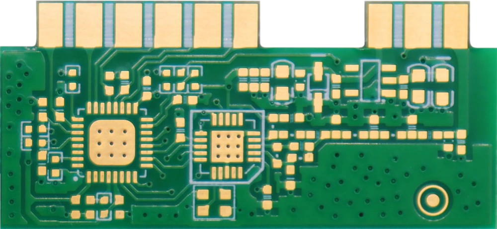
HDI does not replace sound layout practice. A poorly planned HDI stack-up can still suffer from discontinuous reference planes, excessive coupling, poor return paths, or uncontrolled impedance. Review the design requirements through a documented stack-up and impedance-control process rather than selecting HDI solely because the board is small.
4. Mechanical and Thermal Considerations
HDI is primarily an interconnect technology. It does not automatically solve thermal-management problems or mechanical reliability requirements.
Designers must still evaluate:
- Copper distribution
- Thermal vias
- Component heat paths
- Laminate selection
- Coefficient of thermal expansion
- Board stiffness
- Connector loading
- Depanelization stress
- Assembly warpage
In some compact products, HDI reduces board area and frees mechanical space. In other products, a conventional board with more area may provide better thermal spreading, easier assembly access, and lower manufacturing risk.
Material selection should be connected to operating temperature, signal integrity, dielectric behavior, and cost. GreatPCB’s overview of PCB raw materials explains why the laminate decision should be made together with electrical and environmental requirements.
HDI PCB Advantages
More routing capacity in a smaller area
Microvias and build-up layers allow designers to route more connections near dense component footprints. This is particularly useful when a processor, memory device, or BGA has more I/O connections than a conventional via structure can efficiently escape.
Reduced board size and weight
HDI can reduce the area needed for a given function. The result may be a smaller enclosure, a shorter interconnect path, or more functionality within the same product volume.
Better support for fine-pitch components
As package pitch decreases, conventional through-hole vias may block too much of the escape area. Microvia and via-in-pad strategies can provide a more direct escape path, although they require careful pad design, filling, planarization, and inspection.
More flexible layer planning
HDI allows routing to be distributed through build-up layers rather than adding only full-board conventional layers. This can provide a better balance between routing, power, grounding, and signal-integrity needs.
Potentially shorter high-speed connections
Shorter interconnects can reduce via stubs and unnecessary transition length. The actual improvement depends on the complete stack-up and layout, not on the HDI label alone.
HDI PCB Disadvantages
Higher manufacturing complexity
HDI manufacturing may require laser drilling, sequential lamination, microvia plating or filling, tighter layer registration, and additional process inspection.
More demanding design rules
The design team must control pad geometry, microvia placement, copper balance, stack-up, via stacking, solder-mask behavior, and manufacturing tolerances. A design that is electrically valid may still be difficult to fabricate consistently.
Greater sensitivity to process variation
Microvia reliability depends on factors such as dielectric thickness, laser parameters, copper structure, plating quality, via geometry, and thermal cycling. Stacked microvias require especially strong process control because several interconnects are aligned vertically.
More difficult rework
A defective microvia is not repaired in the same way as an accessible through-hole joint. If a problem is detected after lamination or assembly, repair options may be limited and expensive.
Higher tooling and non-recurring cost
HDI may require special laser programs, additional lamination cycles, dedicated process development, and more detailed inspection. These costs can have a greater impact on prototypes and low-volume builds than on stable high-volume production.
When Should You Use an HDI PCB?
HDI is usually justified when one or more of the following conditions apply:
- The component package cannot be routed economically with through-hole vias
- The board must fit a constrained mechanical envelope
- The design has dense BGA, fine-pitch, or high-I/O devices
- Adding conventional layers would create excessive thickness or routing complexity
- Short interconnects are important for signal integrity
- A compact product must integrate more functions without increasing board area
- The design requires build-up layers to separate power, ground, and high-speed routing effectively
Typical HDI PCB applications include:
- Smartphones and compact consumer electronics
- Wearable and portable medical equipment
- Compact cameras and imaging products
- High-density communication modules
- Aerospace and defense electronics with severe packaging constraints
- Advanced automotive control and sensing modules
- High-performance computing and embedded systems
The application list is not a substitute for a design review. A large industrial controller may use conventional multilayer construction even when its electronics are sophisticated. A small sensor module may need HDI despite having relatively few total components.
When Is a Standard PCB the Better Choice?
A conventional PCB may be the better option when:
- The board has adequate routing area
- Component pitch allows normal escape routing
- Through-hole vias do not create unacceptable congestion
- The product is cost-sensitive
- The design needs straightforward inspection and repair
- Thermal or mechanical requirements favor a larger, simpler board
- Production volume does not justify HDI tooling and process development
- The product is in early NPI and the design is likely to change
Choosing standard construction can reduce process risk and simplify sourcing. It may also provide more forgiving design margins during prototype debugging and engineering changes.
The correct comparison is not “advanced versus basic.” It is whether the additional HDI process solves a specific product constraint better than a conventional design.
Is HDI PCB More Expensive?
Usually, an HDI PCB costs more to manufacture than a conventional PCB with similar materials and functionality. The difference comes from process requirements rather than from the name “HDI.”
Major HDI PCB cost factors include:
Layer count and stack-up
More copper layers, build-up layers, and dielectric materials increase fabrication time and material consumption.
Sequential lamination
Each additional lamination cycle adds process time, registration requirements, and inspection points.
Laser drilling and microvia processing
Laser drilling requires dedicated equipment, programming, and control. Microvia plating or filling adds additional process steps.
Material selection
High-Tg, low-loss, thin-dielectric, or specialized laminate systems may cost more than standard FR-4. The material should be selected for the electrical, thermal, and mechanical requirements, not simply to make the board “premium.”
Yield and process margin
Tighter registration, fine-line imaging, microvia reliability, and small annular structures can reduce yield if the design or process window is not well controlled. Scrap and rework are part of the real manufacturing cost.
Tooling and inspection
HDI may require more detailed CAM preparation, laser programs, via inspection, cross-section analysis, electrical testing, and process qualification.
Production volume
A one-time prototype absorbs engineering and tooling costs differently from a repeat production program. A design that is expensive in low volume may become commercially reasonable when the process is stable and the tooling cost is distributed across many boards.
GreatPCB’s article on factors affecting PCB manufacturing and assembly price provides additional context. For procurement, compare the complete cost model rather than only the quoted board price.
How to Control HDI PCB Cost
Cost reduction should preserve the design requirement instead of removing HDI features indiscriminately.
Practical approaches include:
- Use the simplest HDI structure that solves the routing problem
- Avoid stacked microvias when staggered or alternative structures are sufficient
- Reduce unnecessary build-up layers
- Reuse qualified materials and stack-ups where appropriate
- Standardize via and pad geometries
- Review the design with the fabricator before layout is finalized
- Minimize unusual board shapes and special finishes
- Confirm component availability before committing to the design
- Provide test access early in the layout
- Balance copper distribution to reduce warpage and process variation
- Validate prototypes before releasing a high-volume tool set
A DFM review should occur before the layout becomes difficult to change. GreatPCB’s resources on PCB DFM and DFM impact on manufacturing yield are useful references for this stage.
What to Ask an HDI PCB Manufacturer
Before selecting a supplier, ask questions that reveal process control rather than only equipment availability.
Design and engineering
- Can the supplier review the stack-up before layout release?
- How are microvia, via-in-pad, and stacked-via rules defined?
- Can the supplier provide DFM feedback with clear acceptance limits?
- How are registration and copper-balance risks evaluated?
Fabrication
- Which HDI structures are routinely produced?
- How are laser-drilled microvias inspected?
- How are filled vias planarized before subsequent layers?
- How are sequential lamination cycles controlled?
- Is cross-section analysis available for process validation?
Assembly
- Can the assembly line handle the package types on the HDI board?
- How are solder-paste printing and reflow profiles verified?
- Is SPI, AOI, X-ray, or functional testing required for the design?
- How are BGA and via-in-pad soldering risks managed?
Quality and traceability
- What records link material lots to finished boards?
- How are nonconforming boards quarantined and analyzed?
- How are engineering changes and component substitutions approved?
- How long are inspection and test records retained?
GreatPCB’s PCB testing reference covers inspection and testing methods such as ICT, X-ray, electrical testing, and impedance testing.
HDI PCB Selection Checklist
Use HDI when the design problem is primarily one of density, package escape, board area, or interconnect length.
Use standard PCB construction when the design has adequate space and the additional HDI process would not provide a meaningful product benefit.
Before making the final decision, verify:
- Component pitch and escape-routing requirements
- Available board area and thickness
- Required layer count and power-plane arrangement
- Signal-integrity and impedance targets
- Thermal and mechanical constraints
- Material and environmental requirements
- Prototype and production volumes
- Inspection and test coverage
- Supplier process capability
- Total cost, including yield and tooling
Frequently Asked Questions
HDI is better when high interconnect density, compact packaging, fine-pitch component escape, or short routing paths are essential. A standard PCB is better when the design has enough area and the product benefits from lower process complexity, easier inspection, and lower cost. HDI should solve a defined design problem; it is not automatically superior.
The main advantage is higher routing density within a smaller or more constrained board area. Microvias and build-up layers let designers connect dense packages while preserving more usable routing space and improving layer-planning flexibility.
Microvias can be reliable when their geometry, materials, copper structure, plating, and thermal-cycle requirements are properly controlled. Reliability depends on the complete manufacturing process. Stacked microvias and via-in-pad structures require particularly careful design validation and process inspection.
HDI can improve signal integrity by shortening interconnects and reducing some via-related discontinuities. The result still depends on stack-up, reference planes, impedance control, return paths, material properties, and routing quality. HDI alone does not guarantee better electrical performance.
HDI PCB cost is affected by sequential lamination, laser drilling, microvia plating or filling, tighter registration, specialized materials, additional inspection, tooling, and potential yield loss. The final cost depends on the specific stack-up and production volume rather than on a universal HDI surcharge.
Sometimes. If the board has enough routing area, the component pitch is compatible with through-hole or conventional blind-via escape, and the added layers remain acceptable for thickness and cost, a standard multilayer PCB may be the better solution. A fabricator-assisted DFM review can confirm this before the design is finalized.
HDI PCBs are commonly considered for compact mobile electronics, wearables, portable medical devices, communication modules, imaging products, advanced automotive electronics, aerospace systems, and other products where board area or interconnect density is constrained.
GreatPCB supports HDI and standard PCB manufacturing for clients worldwide. Request a global quote or explore our services.
Table of Contents
- Quick Answer: What Is the Difference Between HDI PCB and Standard PCB?
- What Is an HDI PCB?
- What Is a Standard PCB?
- HDI PCB vs. Standard PCB: The Main Engineering Differences
- HDI PCB Advantages
- HDI PCB Disadvantages
- When Should You Use an HDI PCB?
- When Is a Standard PCB the Better Choice?
- Is HDI PCB More Expensive?
- How to Control HDI PCB Cost
- What to Ask an HDI PCB Manufacturer
- HDI PCB Selection Checklist
- Frequently Asked Questions
Tags
Related Posts
PCBA Prototype
September 8, 2026