
Heavy Copper PCB Manufacturing
FR4 standard
Assembly
GreatPCB provides heavy copper PCB manufacturing for power distribution and high-current designs. Share your fabrication files, layer stackup and copper requirements so we can review the construction and prepare a project-specific quotation.
Thicker conductors can reduce resistive loss and help spread heat, but the copper weight must work with the trace geometry, holes, dielectric and assembly process. Our published reference is 4 oz nominal copper for mass production and 6 oz nominal for prototypes. Finished copper thickness, layer allocation and heavy-copper design rules require an approved specification.
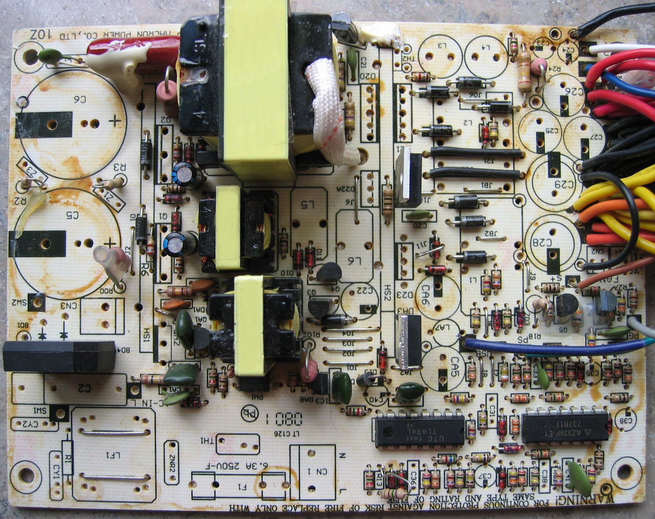
Power-electronics application exampleConductor geometry, connections and heat paths belong in the same review.
What Is Heavy Copper PCB?
A heavy copper PCB uses thicker copper conductors than a conventional circuit board to support demanding power paths. Industry descriptions often start around 3–4 oz, although the term is not used identically by every manufacturer. The useful specification is the copper required on each layer, together with its finished geometry and acceptance criteria.
Copper Weight and Thickness
Copper weight is commonly expressed in ounces per square foot. One ounce of copper spread over one square foot corresponds to approximately 35 µm of thickness; 3 oz, 4 oz and 6 oz are therefore commonly described as about 105 µm, 140 µm and 210 µm respectively. These are approximate nominal conversions, not measurements of the completed board.
Starting foil and finished conductor thickness are different specifications. Depending on the fabrication process, plating can add copper and subsequent processing can remove it. Specify whether a value describes the starting foil, a finished target or a minimum finished thickness, and state the tolerance or acceptance basis. Hole-wall plating needs its own requirement; the copper weight of a surface layer does not define it.
Specify Each Layer
Calling a board “6 oz” leaves important questions unanswered. Identify the layers that need the heavier conductors and those that carry control signals. Different copper weights may be considered within a stackup, subject to engineering review; neither the same weight on every layer nor a particular mixed construction should be assumed.
Use a layer-by-layer copper schedule:
| Specification | Information to Provide |
|---|---|
| Layer identification | Layer number, function and position in the stackup |
| Copper requirement | Starting-foil or finished-copper basis; target or minimum thickness |
| Acceptance basis | Tolerance, measurement location and applicable drawing requirements |
| Plated connections | Separate hole-wall plating requirements and finished-hole dimensions |
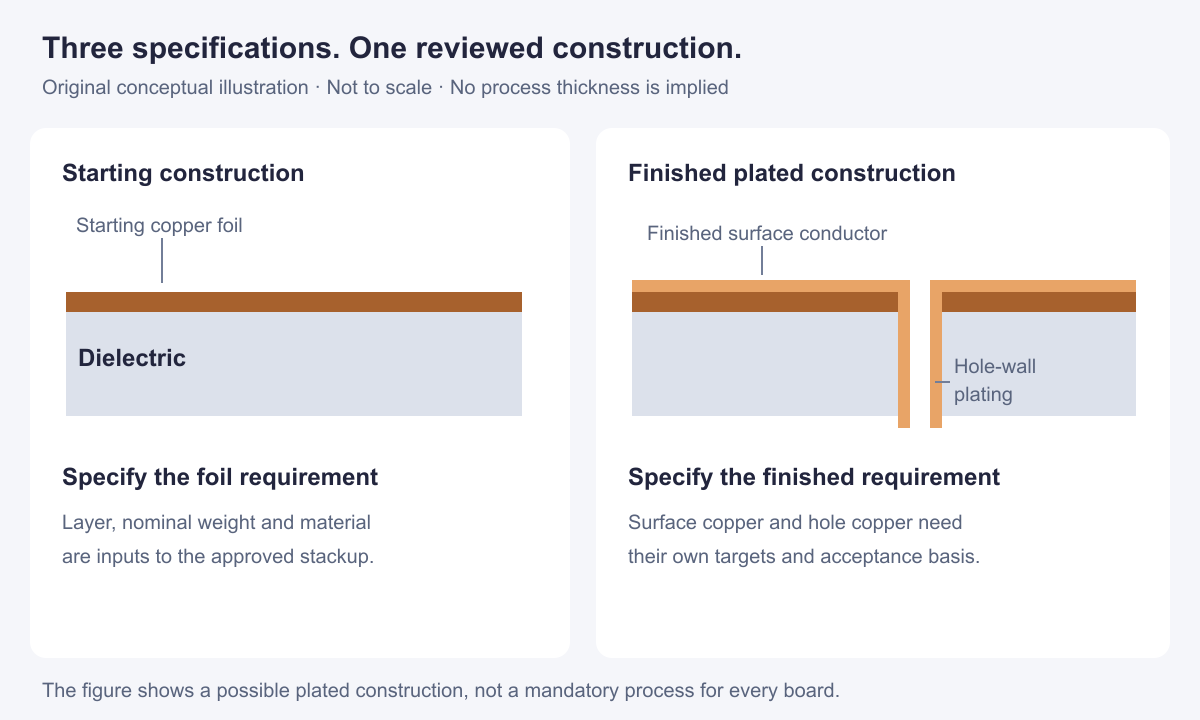
Specify the copper basis and measurement target separately. Conceptual illustration; not to scale.
Manufacturing Capabilities
The table below separates GreatPCB’s published references from the details that need confirmation for a heavy-copper build. Values from a general rigid PCB capability table should not be combined into a promise that every limit is achievable in the same construction.
Copper Specifications
| Item | Published Reference or Available Information | Confirm for Your Project |
|---|---|---|
| Mass-production copper | 4 oz nominal, approximately 140 µm nominal | Specification basis, finished copper and allocation by layer |
| Prototype copper | 6 oz nominal, approximately 210 µm nominal | Proposed construction, finished copper and acceptance requirements |
| Trace width and clearance | Copper-weight-dependent engineering review | Copper thickness, conductor geometry, spacing and local feature density |
| Holes and plated connections | Reviewed against the selected construction | Drill versus finished size, board thickness, layer connections and hole plating |
| Materials | Published material information includes FR-4 options | Actual grade, dielectric construction and thermal/electrical requirements |
| Board thickness | General rigid PCB reference lists a maximum of 8.5 mm | Approved heavy-copper stackup; the general maximum is not a universal heavy-copper limit |
| Manufacturing time | Confirmed in the quotation after engineering review | Files, construction, quantity and inspection requirements |
| Shipping time | Confirmed for the delivery arrangement | Destination, shipping method and dispatch schedule |
For the broader published reference, see our Rigid PCB Capability. Its general 3/3 mil entry and drilling references do not establish design rules for every copper weight.
Materials and Stackup
The stackup defines more than the layer count. Copper pattern, dielectric thickness, resin fill and material properties must work together. A high-Tg material may be appropriate for a project, but Tg alone is not a continuous operating-temperature rating for the completed PCB.
Provide the intended copper schedule and dielectric requirements before finalizing the layout. This allows the material and manufacturing constraints to be considered together, especially where heavier power layers sit beside finer control circuitry. For the broader construction, see our multilayer PCB manufacturing service.
Why Use Heavy Copper?
Heavy copper is useful when the power path needs a larger conductor cross-section within the available board area. Its value comes from the complete design: how current enters, travels through and leaves the board, and how heat reaches the surrounding environment.
Current and Resistive Loss
For the same conductor material, length, width and temperature, thicker copper lowers resistance by increasing cross-sectional area. Lower resistance reduces voltage drop and the heat generated by the same current.
Review the complete path rather than the widest trace alone. Neck-downs, component pads, terminal connections and transitions between layers can constrain a power net. Increasing plane thickness does not automatically resolve a narrow connection or an inadequately specified plated hole.
Thermal Paths and Connections
Copper has high thermal conductivity. Thick conductors and connected copper areas can help distribute heat away from a local source, while appropriately designed plated connections can carry current and link heat-spreading regions.
Good thermal management is crucial for maintaining the performance and lifespan of electronic devices. Heat still needs a route out of the assembly through its materials, mounting arrangement, airflow or cooling interface. More copper is not a substitute for reviewing that route, and it does not guarantee a particular temperature reduction or lifetime.
Design Considerations
Heavy copper changes the manufacturing window. Check the constraints before routing fine features around power areas, rather than selecting a copper weight after the layout is complete.
Trace Width and Clearance
Etching removes copper between the features that remain on the board. It also attacks conductor sidewalls, so the finished trace profile is not necessarily a vertical rectangle. Clearing thicker copper can increase the challenge of controlling lateral removal and narrow gaps. Manufacturing compensation must account for the process and the required final dimensions.
This links copper thickness directly to layout density. A pattern that is manufacturable at a lighter copper weight may need wider features or more clearance at a heavier weight. Share the final copper requirements and tightest routing regions during review. Where the electrical design prevents reducing copper thickness, review spacing, routing or layer allocation together; do not change the copper specification without checking the circuit requirements.
Holes and Plating
Surface conductors and plated holes are separate parts of the current path. Review the drill size, finished-hole size, annular land, board thickness and plating requirement as a connected set of constraints. The finished copper on a power layer does not establish how much copper is present in the hole wall.
Thick copper and the selected stack can also affect drilling and subsequent processing. In pattern-plated constructions, the relationship between plated features and the resist can complicate stripping and isolation between conductors. These are process considerations for the fabricator, not a reason to apply a generic drilling or plating recipe to every heavy-copper design.
Lamination and Copper Balance
Thick inner-layer features leave deeper spaces for dielectric resin to fill. The required resin volume depends on both conductor height and copper coverage, so adding copper thickness without reviewing the prepreg construction can leave an unsuitable fill arrangement.
Material flow, layer registration and cure must suit the stackup. Adding prepreg to supply more resin also changes the construction; it should not be treated as an isolated fix. Review the copper distribution and dielectric thickness together, including regions where sparse and dense patterns meet. The manufacturing process must achieve the intended fill and cured structure without relying on a universal temperature or dwell time.
Thermal and Assembly Requirements
Define continuous and peak current, duty cycle, ambient temperature, allowed temperature rise and the enclosure or cooling arrangement. These conditions affect conductor sizing and the significance of any thermal test. Copper weight alone cannot provide a safe ampere rating for the entire PCB.
Heavy features also create larger steps between copper and substrate. Solder-mask coverage needs attention around conductor edges and deep gaps; a coating that looks acceptable from above may still require a construction-specific coverage assessment.
If assembly is required, include the solder alloy, component limitations and large copper-connected pads in the review. Copper-rich regions can respond differently during heating from smaller nearby features. Develop the soldering profile for the actual board and materials, using measured board/component temperatures where needed. A blanket instruction to increase the peak temperature or extend the process can create problems elsewhere on the assembly.
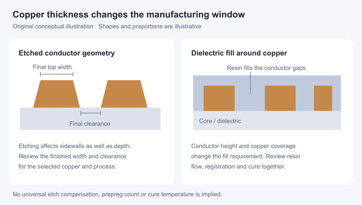
Review final conductor geometry and dielectric fill together. Conceptual illustration; not process limits.
Applications
Power management, industrial controls and automotive electronics can benefit from heavy copper where their power paths require it. The table below connects these applications to the circuit functions and conditions worth reviewing.
| Application | Relevant Power Function | Conditions to Review |
|---|---|---|
| Power converters and supplies | Input/output distribution and switching-stage connections | Current path, allowable loss, conductor geometry and cooling |
| Industrial drives and welding equipment | Motor or load power delivery | Duty cycle, terminals, heat sources and operating environment |
| Renewable-energy and storage systems | Conversion, charging and power distribution | Continuous/peak demand, insulation spacing and thermal path |
| Automotive power electronics | Power delivery in converters, controllers and related circuits | Installation conditions, connections and project-specific qualification |
Choose the construction for the circuit function, not the industry name alone. A communications product may benefit from thick copper in its power supply without requiring thick copper throughout its high-speed signal circuitry. High-voltage clearance, insulation and environmental protection also need their own design review; increased copper thickness does not establish those properties. Our automotive PCB manufacturing and assembly page provides the related project context.
Quality and Inspection
Agree on the inspection scope and acceptance requirements with the manufacturing specification. A useful plan distinguishes conductor geometry, copper thickness, internal construction and electrical connectivity rather than treating “tested” as a complete description. See our PCB testing overview for related bare-board testing information.
Fabrication Checks
Items to discuss include finished conductor width and clearance, copper thickness at agreed locations, plated-hole construction, layer registration, dielectric fill and solder-mask coverage. State which checks, sampling arrangements and records are required for the order.
A microsection can reveal internal copper and plated structures at the selected location. Its value depends on examining the right features and comparing the result with the applicable specification. Define whether acceptance uses a minimum, an average or another agreed measurement basis. A surface thickness reading does not, by itself, demonstrate the condition of every internal layer or plated hole.
Project-Specific Validation
Bare-board connectivity testing and product performance testing answer different questions. Passing an electrical netlist check does not establish the permitted current or temperature rise of the assembled product.
If load testing, thermal measurements, environmental exposure or additional section analysis is needed, state the conditions and requested evidence before quotation. Confirm the scope and availability rather than assuming these tests are included. Representative prototype validation should address the product’s actual current path, connections and cooling conditions.
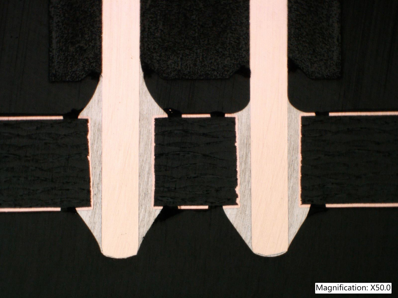
Real PCB-pin microsection example. The photograph does not establish heavy-copper thickness or product acceptance.
Quote Requirements
Clear specifications help separate a manufacturing question from an unresolved design requirement. Send the files together with the conditions that affect the heavy-copper construction.
Files and Specifications
Mark unknowns explicitly. If copper thickness or thermal requirements are still being evaluated, identify them as review items rather than leaving them hidden in a generic “heavy copper PCB” description.
Engineering Review
Submit the project package for review of copper requirements, stackup and manufacturing geometry. Resolve drawing questions and agree on the construction, inspection scope and quotation before release. Where validation is needed, define the prototype build and assessment plan before committing to production.
Request Your Heavy Copper PCB Quote — send the fabrication files and copper schedule to GreatPCB for a project-specific review.