
EV Charging PCB Design: Safety, Power, and Reliability
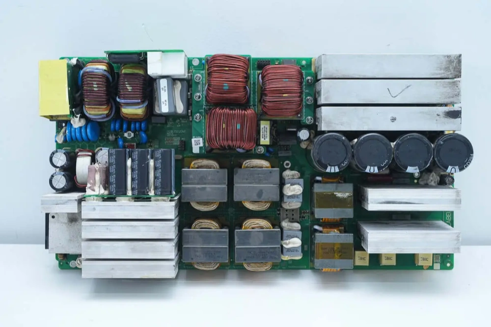
EV charging PCB design is the engineering of a power converter, an insulation system, and a controlled manufacturing process at the same time. The layout must transfer energy efficiently while preserving safe separation between voltage domains, limiting switching noise, removing heat, and allowing every critical connection to be built and tested consistently.
The first design decision is to identify where conversion occurs. An AC charging station can primarily provide switching, protection, metering, and communication while the vehicle's onboard charger converts AC to battery DC. A DC fast charger performs high-power AC-to-DC conversion in the charging equipment itself. These architectures create different PCB constraints even when both are described as "EV charging."
What does a PCB do in an EV charging system?
An EV charging PCB distributes and controls power, measures voltage and current, drives switching devices and contactors, maintains isolation boundaries, and manages communication and safety functions. It may be part of AC electric vehicle supply equipment (EVSE), a vehicle-mounted onboard charger (OBC), or an offboard DC fast charger.
In a charger power stage, the PCB is part of the energy path, not merely a control interface. Its copper resistance affects heat and voltage drop; its loop inductance affects switching overshoot and EMI; its insulation geometry affects leakage and dielectric safety; and its assembly design affects whether a qualified schematic survives production.
| Charging context | Where most AC-to-DC conversion occurs | PCB design emphasis |
|---|---|---|
| AC charging equipment (EVSE) | Usually in the vehicle's OBC; the EVSE manages connection, protection, control, and metering functions | Mains safety, contactor and pilot/control circuitry, surge handling, communication, and serviceability |
| Onboard charger | Inside the vehicle | Typically PFC and isolated DC/DC stages, or an equivalent charger power architecture, with automotive environment, compact thermal paths, EMC, and vehicle interfaces |
| DC fast charger | Inside the offboard charger | High-power rectification/PFC, DC-link management, the specified isolation architecture, current sharing, cooling, metering, and cabinet-level EMC |
This distinction matters during requirements review. A PCB intended for an AC EVSE may have mains-related isolation and contactor-drive constraints but no battery-output power stage. A DC fast charger control or power board must coordinate high-energy conversion, output current sensing, and a larger system of modules, cables, and cooling. An OBC has the additional vehicle environment: vibration, temperature cycling, vehicle-network interfaces, and component qualification requirements.
For context on vehicle-mounted boards, GreatPCB's automotive PCB overview explains why automotive electrical and environmental constraints should be assessed separately from general industrial electronics.
Why EV charging power electronics are difficult to lay out
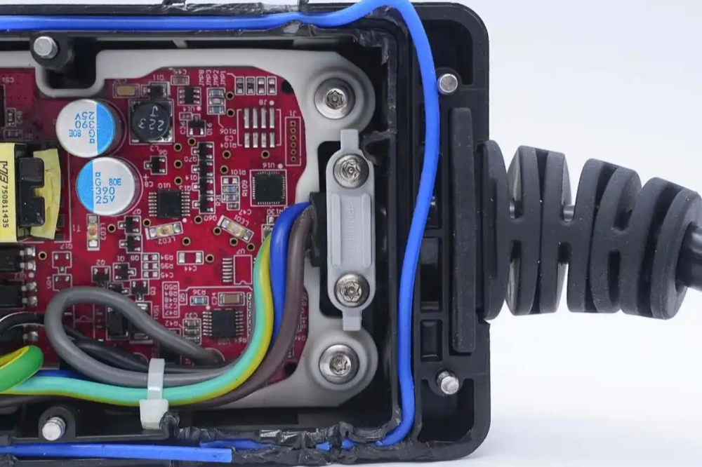
EV charging converters combine high voltage, high current, fast switching edges, low-level measurement, and safety-related isolation on one assembly. The design tension is not simply "make traces wider." Increasing copper area at a high dV/dt switch node can increase its radiating area and parasitic coupling; a larger safety gap can interrupt a return path; and a thermal solution can make soldering or inspection less repeatable.
| PCB design area | What must be controlled | Failure mechanism when it is not controlled |
|---|---|---|
| Power loop | Loop area, copper resistance, inductance, via sharing, and device placement | Switching overshoot, ringing, loss, radiated noise, or local overheating |
| Isolation barrier | Creepage, clearance, material properties, slots, exposed metal, and assembly geometry | Leakage, arcing, dielectric failure, or an invalid safety assessment |
| Measurement and control | Kelvin sensing, reference integrity, filtering, and separation from switch nodes | Incorrect current or voltage readings, unstable control, nuisance trips, or missed faults |
| Thermal path | Device losses, copper spreading, vias, interfaces, airflow or liquid cooling, and sensor location | Component derating, drift, accelerated aging, or thermal shutdown |
| EMC | Differential and common-mode current paths, cable entry, shielding, filter placement, and ground strategy | Failed emissions or immunity tests, communication errors, or control faults |
| Manufacturing | Stack-up, copper balance, stencil design, component spacing, inspection access, and change control | Low yield, inconsistent thermal joints, latent defects, or untraceable field failures |
The right trade-off depends on the actual topology, switching frequency, voltage domain, enclosure, cooling method, and target market. A generic layout rule cannot replace a review of stored energy, transient conditions, and return current at each operating state.
Start with the charging architecture and energy path
Before placing components, draw the complete energy path and mark every voltage domain. In a typical OBC or DC fast charger, the path may include input protection, rectification or active PFC, a DC link, an isolated DC/DC stage, output filtering, contactors, sensing, and a communication/control subsystem. Each stage has different current loops, reference planes, thermal sources, and isolation requirements.
The highest di/dt loops deserve placement priority. In a boost PFC stage, for example, the switching device, diode or synchronous switch, inductor path, and local DC-link capacitors form a loop whose physical area affects inductive voltage overshoot and differential-mode emissions. In an LLC, CLLC, phase-shifted bridge, or other isolated stage, the primary bridge, resonant components, transformer connections, and local capacitors require the same discipline.
Start by placing:
- input and output connectors, fuses, contactors, and current sensors;
- switching devices, gate drivers, local film or ceramic capacitors, and magnetic components around the intended power loop;
- isolation components and the primary-secondary boundary;
- control, sensing, and communications circuits outside high dV/dt regions;
- test points, programming access, inspection clearance, and mechanical supports before routing is dense.
This sequence prevents an all-too-common failure: the control board is laid out first, then the power stage is made to fit around it, creating long switching loops and awkward isolation gaps. GreatPCB's power PCB layout guide is useful background for reviewing loop geometry, component proximity, and return-current paths.
High-voltage and high-current routing
High-current EV charger routing is a path problem, not a trace-width problem. Every neck-down, layer transition, via group, solder joint, connector pin, busbar interface, and return path contributes resistance, inductance, and heat. The limiting point is often not the widest visible copper pour.
Review the full path from source to load, including:
- input or output connector contacts and cable lugs;
- fuses, relays, contactors, shunts, and current sensors;
- copper pours, layer changes, and parallel conductors;
- plated vias, press-fit features, bolts, and busbar interfaces;
- MOSFET, IGBT, diode, or module terminals;
- the intended return path.
Heavy copper can reduce resistive loss, but it changes etching tolerance, copper balance, solder-mask registration, thermal relief behavior, pad geometry, and reflow response. It also does not make a small via array or poorly cooled connector safe. The heavy-copper PCB discussion is a useful companion when deciding whether copper thickness, parallel layers, or a separate busbar is the appropriate current-carrying solution.
Use parallel layers only when the design intentionally transfers current between them. The via pattern must have sufficient electrical and thermal margin for the expected sharing; a large top-layer pour does not automatically distribute current uniformly into an inner layer. For very high current, a busbar, laminated interconnect, or power module connection may be more controllable than forcing all current through PCB copper.
Current sensing and protection routing
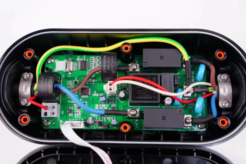
Current sensing drives power regulation, fault detection, metering, and protection. A low-ohmic shunt requires Kelvin connections from the specified sense points so that the voltage drop in load copper, vias, or solder joints is not mistaken for shunt voltage. Keep the differential pair short, symmetrical where the measurement circuit requires it, and away from switch nodes and gate-drive returns.
Hall-effect and fluxgate sensors can measure DC current while providing galvanic separation. A current transformer is suitable only for changing current, such as AC-side measurement or ripple sensing; it cannot measure DC charging output current by itself. For each sensing method, supply decoupling, output reference, filtering, magnetic environment, and connector routing can affect measurement noise and response. Place the sensor based on the fault path it must observe, not only on where board space is available.
Protection circuitry must be designed with the power loop. Gate-drain overshoot, reverse recovery, stray inductance, and the return path of the driver supply influence the actual switching stress. A snubber, clamp, or gate resistor selected in a schematic needs validation on the routed board and in the intended enclosure.
Creepage, clearance, and isolation boundaries
Clearance is the shortest distance through air between conductive parts. Creepage is the shortest distance along an insulating surface. In an EV charger, both are part of the insulation system, together with the material, pollution environment, altitude, transient voltage, isolation class, and any slots or barriers in the PCB and enclosure.
Do not select a universal spacing value from an online example. The design team must define the relevant working voltages and transients, identify the required insulation function, and apply the requirements for the product and market. IEC 60664-1 addresses insulation coordination for equipment within low-voltage supply systems, while IEC 62477-1 addresses general safety requirements for power-electronic converter systems and equipment. Neither turns a copied PCB dimension into a complete product safety case.
Make the primary-secondary or mains-to-safety extra-low-voltage (SELV) boundary visible on both the schematic and every copper layer. Check more than the obvious top-layer gap:
- inner-plane edges and vias near the barrier;
- transformer, optocoupler, digital isolator, and isolated power-supply footprints;
- connector pins, mounting hardware, shields, heat sinks, and test points;
- copper under conformal-coating assumptions;
- solder fillets, flux residue, exposed metal, and assembly tolerances;
- slots, cutouts, panel tabs, and enclosure clearances.
Slots can increase surface distance, but they can also reduce mechanical stiffness, complicate cleaning, and affect fabrication yield. Solder mask is not normally a substitute for a defined insulation barrier unless the applicable product requirements explicitly permit it. Treat the barrier as a system feature that includes the PCB, components, assembly process, enclosure, and contamination environment.
Grounding, return paths, and EMC/EMI control
In EV charging hardware, "ground" may refer to protective earth, chassis, the DC-link negative rail, a primary-side control return, an isolated secondary return, or low-voltage logic reference. These are not interchangeable. A grounding strategy must specify which currents use each reference and where they are intentionally connected. This directly affects electromagnetic compatibility (EMC) and electromagnetic interference (EMI).
The two main noise mechanisms should be assessed separately:
- Differential-mode noise circulates in an intended conductor loop. Reduce it by making the switching loop compact, controlling edge rates, and placing differential filters in the path they are intended to affect.
- Common-mode noise flows through parasitic capacitances and returns through chassis, protective earth, cable shields, transformer capacitance, or other references. It is strongly affected by cable entry, isolation geometry, Y-capacitor strategy where applicable, shielding, and enclosure bonding.
Do not split a reference plane under a fast control or communication route unless the return path has been deliberately provided. A fast signal crossing a gap often takes a larger, less predictable return path, increasing loop inductance and coupling. Conversely, do not extend a quiet reference plane across an isolation barrier merely to make routing convenient.
Place noisy switch nodes away from current-sense amplifiers, isolated feedback lines, pilot/control circuits, and communications interfaces. Route gate-drive loops close to their devices, with local decoupling at the driver supply pins. Position surge protection and interface filtering at the connector entry where they can control the current before it spreads through the board.
The PCB stack-up affects field containment, impedance, and return-path continuity. GreatPCB's stack-up and EMC article and impedance-control guide explain why a nominal trace width alone is not enough for a controlled interconnect. For CAN, Ethernet, power-line communication (PLC), or other fast links, use the actual dielectric thickness, copper geometry, and reference structure agreed with the fabricator.
Thermal design for charger power stages
Thermal performance is determined by the complete path from semiconductor junction to ambient or coolant, not by copper area alone. The highest loss components often include switching devices, diodes, magnetic components, shunts, DC-link capacitors, gate-drive supplies, and contactor or relay drivers. Their temperatures also influence measurement accuracy and component life.
Thermal design should answer four questions:
- What losses occur in every operating mode, including low-line, high-line, peak output, standby, fault response, and elevated ambient conditions?
- How does heat move through the package, solder joint, copper, thermal vias, dielectric, heat sink, chassis, airflow, or liquid-cooling interface?
- Which components are thermally coupled in a way that affects control accuracy, capacitor life, or derating?
- Where are temperature sensors relative to the actual limiting junctions and magnetic hot spots?
Thermal vias under a power package can reduce spreading resistance when the component land pattern and assembly process support them. They do not replace a defined thermal interface or enough copper. Via filling, tenting, solder-mask treatment, and stencil aperture can change solder wicking and voiding, so the thermal solution must be reviewed with assembly in mind.
Keep heat-producing parts away from temperature references, precision current-sense amplifiers, and electrolytic or polymer capacitors whose life is temperature-sensitive. A sensor mounted on a cool copper region may report a reassuring board temperature while the adjacent semiconductor junction is limiting. For a wider review of power density, copper, and heat paths, see GreatPCB's high-power PCB heat-management article.
Stack-up, copper thickness, and material selection
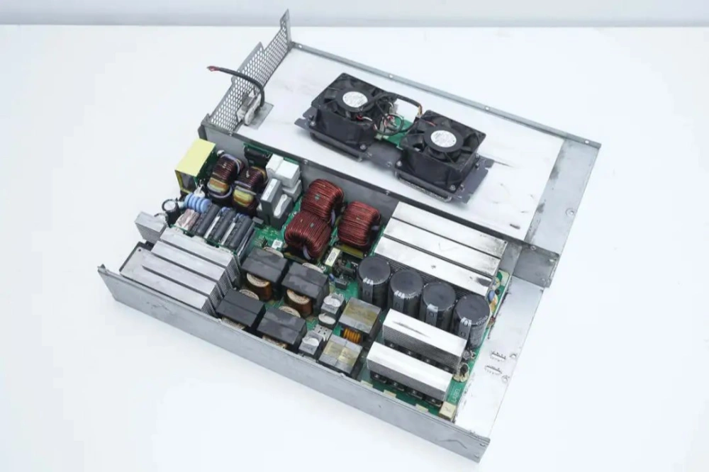
The stack-up is an electrical, thermal, safety, and manufacturing decision. It defines the dielectric spacing that affects controlled impedance and plane capacitance, the location of return paths, the available copper cross-section, the construction around isolation barriers, and the mechanical behavior of the board.
Choose the construction based on actual requirements, including:
- copper thickness, finished copper, and etching tolerance on each layer;
- dielectric thickness and resin system around high-voltage and high dV/dt regions;
- z-axis expansion and plated-hole reliability under thermal cycling;
- comparative tracking index (CTI) and moisture behavior where the insulation design depends on surface performance;
- copper balance, warpage risk, and the package thermal path;
- availability, material traceability, and compatibility with the planned soldering and cleaning process.
High-Tg FR-4 can provide useful process and thermal margin, but it is not a complete material specification and does not make a charger board inherently reliable. The resin system, glass construction, copper adhesion, moisture performance, dielectric thickness, and end-use environment still matter. GreatPCB's PCB materials overview is useful for comparing the roles of FR-4, aluminum, ceramic, and other board material families.
More layers can make an EV charger PCB easier to control by providing short power loops, contiguous references for control signals, and routing space that avoids forcing safety boundaries into awkward locations. More layers also add lamination interfaces, cost, via choices, and fabrication variables. The correct layer count is the one that makes the electrical, insulation, thermal, and yield requirements controllable.
DFM and PCB assembly (PCBA) considerations
Design for manufacturability (DFM) and design for assembly (DFA) for EV charging boards begin before the layout is frozen. The fabricator and assembler need the real stack-up, copper weights, slot geometry, hole structure, surface finish, package list, thermal requirements, and test strategy. A generic design-rule check cannot assess the combined effect of heavy copper, high-voltage separation, large thermal pads, magnetics, and high-mass interconnects.
Key DFM and DFA checks include:
- whether fine features remain manufacturable beside heavy copper or wide pours;
- whether annular rings, via aspect ratio, copper plating, and via fields support the current and thermal path;
- whether creepage slots, routs, and break-off tabs preserve the intended barrier after fabrication and depanelization;
- whether board thickness and copper balance limit warpage through reflow or selective soldering;
- whether large exposed pads have a defined stencil aperture, paste-volume target, and voiding acceptance method;
- whether tall magnetics, heat sinks, relays, connectors, and busbar interfaces are mechanically supported;
- whether critical components have controlled alternates with equivalent electrical, thermal, safety, timing, and package behavior;
- whether test points, isolation verification access, programming, and functional-test connections remain accessible after assembly.
GreatPCB's DFM and final-yield guide provides useful background on carrying manufacturing limits into the design release. The practical output should be an agreed stack-up and process window, not a one-time approval label.
During PCBA, solder-paste printing, solder-paste inspection (SPI), component placement, reflow profiling, selective soldering where needed, automated optical inspection (AOI), X-ray where it can inspect a concealed joint, in-circuit testing (ICT), and functional testing each detect different failure modes. A void or poorly wetted thermal pad can change a device's thermal path; a shifted shunt or current-sense resistor can alter measurement accuracy; and flux residue around an insulation boundary can matter in a high-voltage product. GreatPCB's PCBA test-method overview explains the different roles of ICT, AOI, functional testing, and related inspection methods.
Need support with EV charging PCB design, heavy copper, isolation, or DFM? FLJPCB offers global PCB manufacturing and assembly services.
Testing and reliability: link design intent to production evidence
Inspection is not the same as verification. AOI can identify visible placement and solder defects; X-ray can help inspect hidden joints and some voids; ICT can confirm many nets and component values. None of those methods alone proves switching performance, EMC, isolation, thermal margin, charging behavior, or product safety.
Build a control plan that links each design characteristic to evidence. For example, the released stack-up and material record support insulation and impedance assumptions; reflow profiles and SPI data support solder-process consistency; functional tests support control, sensing, and communication behavior; and the appropriate dielectric, insulation-resistance, transient, thermal, and EMC tests support the relevant product requirements.
| Manufacturing or verification control | What it helps establish | What it cannot establish alone |
|---|---|---|
| Material and stack-up records | Approved construction, dielectric geometry, copper weights, and lot traceability | That the finished charger meets every safety and EMC requirement |
| Cross-sections, coupons, and dimensional checks | Plating, hole structure, registration, and selected fabrication characteristics | System-level current sharing or thermal performance in the enclosure |
| SPI, placement records, AOI, and X-ray where justified | Paste, component-placement, visible solder, and some hidden-joint evidence | Converter efficiency, isolation behavior, or long-term environmental reliability |
| ICT, boundary scan, and functional test | Connectivity, programming, selected analog limits, control behavior, and communications | Full-load thermal, transient, dielectric, or EMC margins unless those are explicitly tested |
| Change control and traceability | The ability to relate a production unit to material, assembly, test, and revision records | That an unreviewed substitution is technically equivalent |
The reliability plan must match the product. An OBC may require a vehicle-specific environmental and component-qualification approach, while an offboard charger requires its own duty cycle, enclosure, grid, cable, and service assumptions. Temperature cycling, humidity, vibration, surge and transient exposure, contamination, and repeated connection cycles cannot be replaced by a room-temperature bench test.
Standards: keep their scopes separate
Standards guide requirements and verification, but none of the following labels makes a PCB automatically compliant, safe, or suitable for every charger. The applicable edition, market, product architecture, installation environment, and customer specification determine the actual requirement set.
| Standard or specification | Relevant scope | What it does not prove by itself |
|---|---|---|
| IEC 61851-1 | General requirements for conductive EV charging systems | That a particular PCB layout, charger, or installation is compliant in every market |
| IEC 62477-1 | General safety requirements for power-electronic converter systems and equipment | That copied creepage values or a component selection completes the converter safety assessment |
| IEC 60664-1 | Principles, requirements, and tests for insulation coordination within low-voltage supply systems | A universal PCB spacing value without the actual voltage, transient, pollution, material, and altitude conditions |
| IPC standards | PCB design, fabrication, assembly acceptability, and test-method documents, depending on the document selected | Charger-level electrical safety, EV charging interoperability, EMC, or field reliability |
| IATF 16949 | Automotive quality-management requirements for relevant production organizations and processes | That an individual OBC PCB meets electrical performance or functional-safety requirements |
| AEC-Q100 and AEC-Q200 | Stress-test qualification documents for automotive ICs and passive components, respectively | That the complete vehicle charger, PCB layout, or system has been qualified |
For conductive charging equipment, IEC 61851-1 provides system-level context, not a PCB layout rulebook. For vehicle-mounted chargers, component qualification, manufacturing quality systems, board workmanship, converter safety, and system validation are related evidence streams, not substitutes for one another.
Common EV charging PCB design mistakes
These mistakes often survive an early prototype because the board is tested at reduced power, without its final enclosure, or without the actual cable and grid environment:
- treating every AC charging station as though it contains the same power-conversion stages as a DC fast charger;
- routing high-current copper generously but leaving a narrow via field, connector pin, shunt joint, or thermal neck-down as the real limit;
- placing the local high-frequency DC-link or commutation capacitor too far from the switching bridge and relying on a wide copper pour to compensate;
- using a generic creepage or clearance dimension without confirming insulation class, transients, pollution, altitude, material, and applicable requirements;
- checking the top-layer isolation gap but missing inner-layer copper, hardware, test points, or solder fillets near the barrier;
- sharing high-current return copper with shunt sensing, gate-drive return, or low-level analog measurement;
- treating protective earth, chassis, primary return, and logic ground as one net without defining actual current paths;
- putting common-mode filtering near the controller instead of at the cable or power-entry boundary where the noise path begins;
- selecting high-Tg laminate or heavy copper as a shortcut for the broader thermal, insulation, and manufacturing review;
- using AOI or a passing functional test as proof of dielectric, EMC, or full-load thermal performance;
- approving an alternate component without confirming its package, parasitics, thermal behavior, isolation rating, timing, and qualification status.
EV charging PCB design checklist
Before release, the design team should be able to answer these questions:
- Is the board for AC EVSE control, an onboard charger, a DC fast charger, or a defined subsystem within one of them?
- Where does each voltage domain begin and end, and where does power conversion occur?
- Have normal, transient, and fault voltages been defined across every insulation boundary?
- Have creepage and clearance been assessed for the actual insulation function, environment, and governing requirements?
- Are the PFC, bridge, DC-link, resonant, and output-current loops physically short and intentionally routed?
- Are shunt and voltage-sense connections Kelvin routed and kept away from high dV/dt and high di/dt paths?
- Are protective earth, chassis, primary return, isolated output return, and logic references assigned clear current paths?
- Are thermal paths defined from each limiting device to the intended heat sink, chassis, airflow, or coolant interface?
- Is the stack-up based on real dielectric thickness, finished copper, and material data rather than nominal assumptions?
- Have cable entry, shields, surge protection, differential filtering, and common-mode paths been reviewed together?
- Has the fabricator reviewed heavy copper, via structure, slots, copper balance, surface finish, and panelization?
- Are stencil design, reflow profile, selective-solder requirements, inspection coverage, and rework limits defined for the power devices and magnetics?
- Do production records control component substitutions, material lots, firmware, test limits, and deviations together?
- Does the verification plan cover full power, intended cooling, cable configuration, enclosure, transient, insulation, EMC, and environmental conditions?
FAQ: EV charging PCB design
An EV charging PCB is a circuit board used to control, measure, protect, or convert power in EV charging equipment. It can be part of an AC EVSE, vehicle onboard charger, or DC fast charger. Its design must manage high-voltage isolation, switching power loops, sensing, thermal paths, EMC, and manufacturing consistency.
An AC EVSE PCB commonly handles connection control, protection, metering, and charging communication while the vehicle's onboard charger converts AC to battery DC. An onboard charger PCB contains the AC-to-DC power electronics, typically including PFC and isolated DC/DC conversion, so its power-loop, thermal, and automotive-environment requirements are usually more demanding.
A DC fast charger performs high-power conversion in the offboard charger. Its PCBs must manage rectification or PFC, DC-link energy, isolated output conversion, high output current, module coordination, cabinet cooling, cable effects, and system EMC. The design must be reviewed with the complete charger and not as an isolated control board.
Creepage and clearance help prevent leakage, arcing, and insulation breakdown between conductive parts at different potentials. Clearance is through air; creepage follows the insulating surface. Required distances depend on voltage, transients, pollution, material, altitude, and insulation function, so a copied spacing number is not a valid design basis.
Layout changes EMI by changing switching-loop area, parasitic inductance, return paths, and coupling to cables, chassis, and sensitive circuits. Compact power loops reduce differential-mode emissions. Controlled cable-entry filtering, shielding, isolation geometry, and chassis paths help manage common-mode noise.
Many EV charger boards use FR-4-based multilayer constructions, but the suitable material is selected from the voltage, temperature, thermal path, dielectric thickness, z-axis expansion, moisture behavior, copper weight, and manufacturing process. Higher Tg may add margin, but it does not by itself establish safety or reliability.
Review the complete path through connectors, fuses, shunts, switches, copper pours, vias, solder joints, and return conductors. Use enough copper cross-section and intentionally designed layer transitions, but also identify bottlenecks and heat sources. For some current levels, a busbar or power-module interface is more appropriate than adding more PCB copper.
PCBA affects reliability through solder-joint quality, thermal-pad voiding, component placement, residue near insulation barriers, material traceability, and process consistency. SPI, reflow profiling, AOI, X-ray where useful, electrical testing, and functional testing each cover different defects. Their results should be tied to controlled revisions and the product verification plan.
Table of Contents
- Yintoni eyenziwa yi-PCB kwinkqubo yokutshaja ye-EV?
- Kutheni kunzima ukucacisa amandla okutshaja kwe-elektroniki kwi-EV
- Qala ngoyilo lokutshaja kunye nendlela yamandla
- Indlela yokuqhuba umbane ophezulu kunye nombane ophezulu
- Imida yokuqhekeka, yokucoca, kunye neyokwahlukanisa
- Ukumisa umhlaba, iindlela zokubuyela umva, kunye nolawulo lwe-EMC/EMI
- Uyilo olushushu lwamanqanaba ombane wetshaja
- Ukufakwa kwee-stack, ubukhulu be-copper, kunye nokukhethwa kwezinto
- Izinto eziqwalaselwayo kwi-DFM kunye ne-PCB assembly (PCBA)
- Uvavanyo kunye nokuthembeka: qhagamshela injongo yoyilo nobungqina bemveliso
- Imigangatho: gcina ii-scopes zabo zahlukile
- Iimpazamo zoyilo lwePCB zokutshaja i-EV eziqhelekileyo
- Uluhlu lokuhlola uyilo lwe-PCB yokutshaja i-EV
- Imibuzo Ebuzwa Rhoqo: Uyilo lwePCB yokutshaja i-EV
Related Posts
PCBA Prototype
July 21, 2026
PCBA Prototype
July 17, 2026