
Automotive BMS PCB Design: Key Engineering Considerations
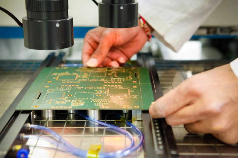
PCB design for an automotive battery management system (BMS) must keep high-energy battery paths, precision measurement circuits, communications, thermal loads, and safety barriers predictable over the product life. The board is not just a carrier for a battery-monitoring IC. Its copper geometry, return paths, insulation distances, component placement, materials, and manufacturing controls directly affect cell-voltage accuracy, fault detection, EMC, heat, and service reliability.
The most useful design sequence is to define the BMS architecture and safety boundaries first, then place the sensing and protection functions, partition noisy power circuits, set the stack-up and isolation geometry, and only then optimize routing and manufacturing cost. A PCB that passes a bench functional test can still fail in a vehicle because of switching transients, vibration, temperature cycling, contamination, or production variation.
What is a BMS PCB?
A BMS PCB is the printed circuit board that measures battery cells and pack conditions, processes those measurements, controls protection and balancing functions, and communicates status to the vehicle or battery controller. Depending on the architecture, one board may monitor an entire pack, or several cell-monitoring boards may report to a central controller through an isolated communication link.
A typical automotive BMS can contain:
- a cell-monitoring analog front end (AFE) and multiplexer or ADC;
- a microcontroller for measurement, diagnostics, state estimation, and communications;
- voltage, current, and temperature sensing circuits;
- passive or active cell-balancing paths;
- contactor, pre-charge, fuse, and discharge-control interfaces;
- isolated or non-isolated power conversion;
- CAN or CAN FD, and sometimes other vehicle-network interfaces;
- protection against overvoltage, undervoltage, overcurrent, short circuit, and insulation faults.
The exact partition depends on pack voltage, cell count, isolation architecture, service strategy, and the system safety concept. A low-voltage 12 V battery controller and a high-voltage traction-battery BMS do not impose the same PCB constraints.
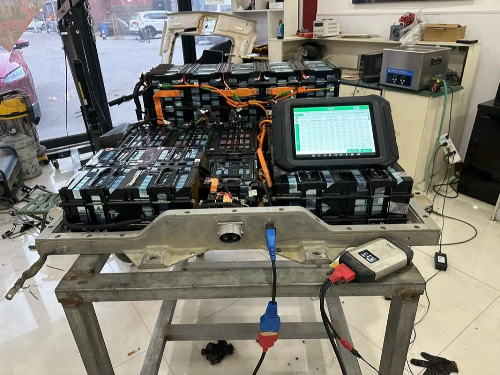
Why is automotive BMS PCB design different?
Automotive BMS boards combine precision analog measurement with high-energy switching and long-term environmental exposure. The voltage difference between adjacent cell taps may be modest, while the pack-to-chassis potential can be hazardous. At the same time, a few millivolts of measurement error can affect balancing or state-of-charge calculations, and a noisy switching node can corrupt a measurement that otherwise looks correct in a schematic.
The main design tension is therefore isolation and noise control without making the board impossible to manufacture or inspect. The design has to control:
| Design area | What must be controlled | Typical failure if it is ignored |
|---|---|---|
| Cell and current measurement | Kelvin connections, filter matching, reference integrity, and return paths | False cell fault, inaccurate state estimation, or missed overcurrent event |
| High-current switching | Copper cross-section, via current sharing, loop area, and thermal spreading | Excessive temperature rise, voltage drop, or damaged MOSFET and shunt connections |
| HV/LV separation | Creepage, clearance, slots, contamination control, and isolation components | Insulation breakdown, leakage, arcing, or unsafe diagnostic behavior |
| EMC and communications | Current loops, cable entry, common-mode paths, filtering, and reference planes | CAN errors, radiated emissions, or susceptibility to inverter transients |
| Thermal design | Heat sources, copper spreaders, thermal vias, and sensor placement | Drift, accelerated aging, or thermal shutdown |
| Manufacturing | Stack-up capability, solderability, inspection access, and change control | Low yield, intermittent faults, or boards that pass inspection but fail in service |
For general automotive PCB background, see GreatPCB’s overview of automotive PCB differences and applications. The BMS-specific requirements below should still be derived from the battery system, not copied from a generic automotive board.
FLJPCB supports PCB manufacturing and assembly for automotive BMS and other high-reliability applications worldwide.
Electrical design considerations
Cell-voltage measurement
Cell-voltage inputs are high-impedance, noise-sensitive measurement nodes. Route each cell tap as a defined pair or according to the selected AFE vendor’s reference layout and input guidance, with protection and filtering placed close to the device. Keep the input components matched where the measurement method depends on differential accuracy. A long, unbalanced route can pick up switching noise or create unequal RC settling that appears as a cell-voltage error.
The input network must also tolerate the fault conditions specified by the AFE and battery architecture. Series resistors, clamps, fuses, and filter capacitors should be selected as a coordinated protection network. A protection component that survives a transient electrically may still add leakage, capacitance, or recovery behavior that distorts the measurement.
Do not route cell-tap traces through the return path of a balancing resistor, contactor coil, DC/DC converter, or gate driver. If a cell-monitoring IC uses a local reference or isolated ground, follow the vendor’s reference plane and decoupling strategy rather than applying a generic “analog ground” rule.
Current sensing
Current sensing may use a shunt resistor, Hall-effect sensor, fluxgate sensor, or another isolated transducer. For a shunt, the sense connections should be Kelvin routed from the intended sensing points, separate from the high-current copper path. If the sense pair shares copper with load current, the voltage drop in that copper becomes part of the measurement and changes with temperature and assembly variation.
Place the shunt, amplifier or AFE input, protection parts, and filter network so the differential loop is short and symmetrical. Keep high dV/dt switch nodes away from the sense pair. Also account for thermoelectric offsets and resistor self-heating: a current-sense layout can be electrically symmetrical and still drift if one side has a different thermal environment.
Cell balancing
Passive balancing converts excess cell energy into heat, usually through a resistor and a switching device. The PCB must provide a controlled thermal path from the balancing resistor and MOSFET into copper and, where appropriate, thermal vias or a chassis interface. Keep balancing currents out of the cell-measurement return path, and verify that the AFE input protection and filter components tolerate the balancing waveform.
Active balancing introduces additional inductors, switches, and high-frequency current loops. Its control and power paths need the same placement discipline as a small power converter. The balancing strategy also affects how many channels can operate at once, which changes the board’s worst-case thermal condition.
Protection and contactor control
Contactor coils and switching in pre-charge, discharge, and fuse paths can generate large transients. Place suppression components close to the coil or switching device, and give their return current a path that does not cross the analog measurement area. Gate-driver and MOSFET protection should be considered together with the power-stage loop inductance; a schematic-level snubber value does not guarantee the same result after routing.
The BMS PCB should make abnormal states diagnosable. Test points, current-sense access, isolation-barrier visibility, and connector keying can reduce ambiguity during end-of-line testing and service without compromising the insulation boundary.
High-current routing and power integrity
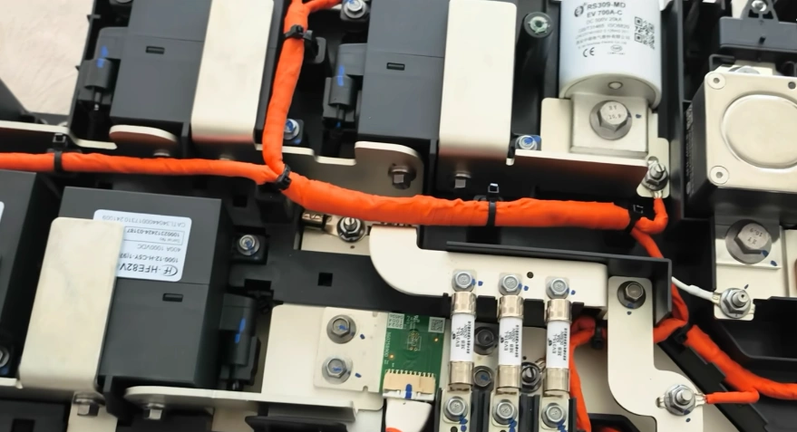
High-current BMS paths are governed by resistance, inductance, temperature rise, and mechanical current-transfer points. Increasing copper thickness can reduce resistance, but it does not automatically solve a narrow neck-down, a small via field, a weak connector contact, or a poorly cooled MOSFET.
Use the complete path to review:
- battery or bus connector;
- fuse, shunt, contactor, or switching device;
- copper pours and layer transitions;
- vias, press-fit or bolted interfaces;
- return path to the opposite connector.
Parallel copper layers can share current when the vias and transitions are designed for that purpose. Do not assume that a large top-layer pour transfers current uniformly into an internal plane. Via diameter, pitch, barrel resistance, solder fill, and thermal conditions all affect sharing.
The GreatPCB power PCB layout guide provides useful background on placing power conversion close to its load and controlling loop length. For BMS work, extend that review to the shunt, contactor driver, balancing circuits, connector pins, and isolation boundary.
Heavy copper may be appropriate for a high-current path, but it changes etching, solder-mask registration, pad geometry, thermal balance, and assembly conditions. The final choice should be made with the fabricator during DFM. GreatPCB’s high-power PCB heat-management discussion is a related reference, not a substitute for a calculated temperature-rise and current-path review.
Creepage, clearance, and isolation
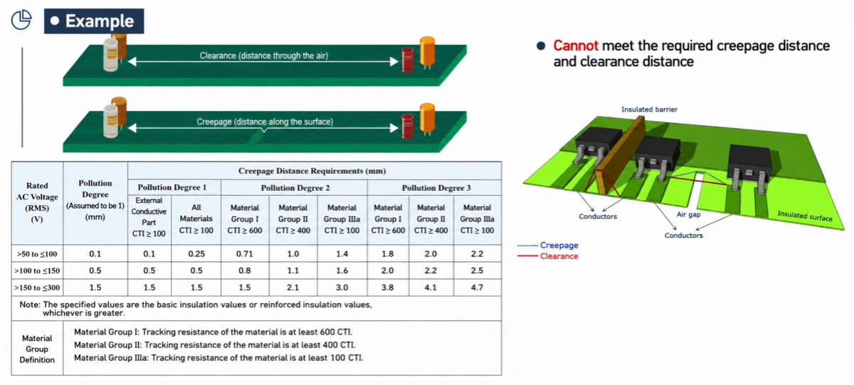
Clearance is the shortest distance through air between conductive parts. Creepage is the distance along an insulating surface. Both matter on a BMS PCB, but the required distance depends on working voltage, transient overvoltage, pollution degree, material properties, altitude, insulation class, and the applicable system or OEM requirements.
Do not choose a single spacing value because it is common on another board. Define the isolation boundary on the schematic and PCB, then check every crossing:
- cell-tap domains to low-voltage logic;
- pack positive or negative to chassis-referenced circuitry;
- isolated CAN or daisy-chain interfaces;
- isolated DC/DC converter primary and secondary sides;
- connector pins, mounting hardware, shields, and test points;
- copper pours, vias, thermal pads, and exposed metal near the barrier.
Slots or cutouts can increase creepage, but they also affect mechanical strength, routing, manufacturing, cleaning, and enclosure sealing. A slot is useful only when it is included in the insulation design and can be fabricated consistently. Solder mask is not normally treated as the sole safety barrier unless the governing requirement explicitly allows it.
Keep the isolation boundary visible in the layout review. Avoid copper islands that unintentionally bridge the barrier, and check internal layers as carefully as the top and bottom layers. Contamination and moisture can reduce surface insulation resistance, so the board finish, cleaning process, conformal-coating assumptions, and enclosure environment belong in the same review.
Grounding, return paths, and signal integrity
Grounding is not solved by labeling every net “GND.” The design team must identify where switching current, sensor return current, communication return current, and chassis or shield current flow at each operating state.
Useful practices include:
- keep the AFE reference and decoupling loop compact;
- route differential sense pairs together and away from high-current edges;
- keep high di/dt loops small and local to their switching devices;
- avoid splitting a reference plane beneath a fast signal unless the return path is intentionally redirected;
- connect power and signal grounds at defined locations that match the isolation architecture;
- place common-mode chokes, termination, and transient protection at the communication entry point when the network design calls for them.
CAN and CAN FD are differential buses, but the PCB still affects their common-mode behavior. Termination belongs to the network topology, not simply to every board, and the transceiver’s supply and reference currents need a controlled path. For impedance-controlled or high-speed portions of the design, use the actual dielectric thickness and copper geometry in the stack-up calculation. GreatPCB’s impedance-control explanation gives a useful overview of why a nominal trace width is not the same as a controlled impedance.
Thermal management
The BMS thermal problem is local as well as global. MOSFET conduction and switching losses, shunt heating, balancing resistors, linear regulators, isolated power converters, and contactor drivers can create different hot spots on the same board.
Thermal design should answer four questions:
- Where is the heat generated at the worst electrical load and balancing state?
- How does it move through copper, vias, the board, the enclosure, and any thermal interface?
- Where are temperature sensors located relative to the actual hot spots?
- How does temperature change measurement accuracy, resistance, timing, and component life?
Thermal vias under a power package can reduce spreading resistance when the package and assembly process support them. They are not a replacement for adequate copper area or a defined heat path. A temperature sensor placed several centimeters from a shunt or MOSFET may report a plausible board temperature while missing the component junction’s limiting condition.
The stack-up, copper weight, solder-mask openings, thermal reliefs, and enclosure mounting should be reviewed together. A large copper pour may improve heat spreading but also increase solder imbalance or couple switching noise into a sensitive region.
EMC and EMI control
BMS boards encounter noise from DC/DC converters, gate drivers, contactor coils, inverters, motors, and long battery and vehicle harnesses. The design objective is both to reduce emissions and to prevent noise from becoming a false battery fault.
Separate the mechanisms:
- Differential-mode noise is associated with voltage between conductors in a loop and is reduced by shortening the loop, controlling switching edges, and filtering the intended path.
- Common-mode noise appears together on conductors relative to a reference such as chassis and is strongly affected by parasitic capacitance, cable shields, isolation barriers, and return paths.
Start EMC work with current loops and parasitic capacitance, not with a last-minute shield. Place input filters at the connector, keep switch-node copper compact, provide a continuous reference where high-speed signals need it, and prevent sensitive cell-tap routes from running beside power transitions. A stack-up can help control field coupling and return paths; GreatPCB’s PCB stack-up and EMC article provides related background.
Filter components also need a defined purpose. A capacitor added to a cell input changes the AFE settling time and can interact with the source impedance. A common-mode choke on CAN can improve emissions in one harness configuration and create unwanted resonance or signal distortion in another. Validate the filter with the actual transceiver, harness, enclosure, and test setup.
Component placement and PCB layout sequence
Placement should follow current and information flow:
- place cell connectors and the cell-monitoring AFE so tap routes are short and orderly;
- place the current sensor and its amplifier at the sensing points;
- place protection, contactor, and pre-charge drivers near their connectors and power devices;
- place the MCU and communications interface away from high dV/dt nodes but close enough to keep control and bus routes short;
- place decoupling at each IC supply pin and keep the loop area small;
- reserve test points and inspection access before filling the remaining space.
Avoid routing by convenience. A cell-tap trace that takes a quiet path on the schematic may cross a gate-drive return on the PCB. Review the layout in operating states: charge, discharge, balancing, contactor switching, wake-up, sleep, fault, and service. The best route in steady state may be the wrong route during a contactor transient.
PCB material, stack-up, and copper thickness
The material decision should follow voltage, temperature, mechanical, EMC, and manufacturing requirements. Standard FR-4 may be suitable for many BMS boards, but the exact resin system, glass construction, dielectric thickness, moisture behavior, and thermal expansion still matter. A higher-Tg laminate can provide more process and thermal margin, but Tg alone does not establish the board’s reliability.
Review at least:
- dielectric thickness and its effect on creepage, clearance, and controlled impedance;
- z-axis expansion near plated holes and layer transitions;
- in-plane thermal spreading and copper weight;
- moisture absorption and insulation resistance in the intended environment;
- compatibility with soldering, cleaning, coating, and rework;
- material availability and lot traceability.
Use a multilayer stack-up when it provides a defined reference plane, shorter power loops, better analog separation, or more reliable current sharing. More layers also create more interfaces, vias, and manufacturing decisions. Layer count should be justified by electrical, thermal, isolation, and yield requirements rather than used as a generic quality signal.
Design for manufacturing and assembly
DFM must start while the BMS architecture is still changeable. Ask the fabricator to review the actual stack-up, copper weights, minimum spacing, hole structure, isolation slots, panelization, and finish. A generic design-rule file cannot capture every issue created by heavy copper, mixed technologies, large thermal pads, or an isolation barrier.
Important DFM/DFA checks include:
- whether the chosen copper thickness can be etched with the required fine features;
- whether via aspect ratio, annular ring, and thermal-via fields are within the process window;
- whether isolation slots can be routed and inspected without weakening the panel;
- whether component spacing supports stencil printing, placement, AOI, and rework;
- whether large copper pads need a defined stencil aperture or thermal-relief strategy;
- whether connectors and heavy components are supported against vibration and board flex;
- whether test points are accessible for ICT, boundary scan, programming, and functional tests;
- whether critical ICs, shunts, connectors, and isolation parts have a controlled sourcing plan, approved alternates, and lifecycle monitoring;
- whether every proposed alternate has the same electrical, thermal, safety, timing, package behavior, and qualification status.
GreatPCB’s PCB DFM and final-yield guide is relevant to the handoff between design intent and fabrication constraints. DFM approval should record the agreed limits; it should not be treated as a one-time checkbox.
During PCBA, surface-mount technology (SMT) processes such as solder-paste printing, SPI, component placement, and reflow profiling, together with AOI, X-ray where justified, in-circuit or boundary-scan testing, and functional testing, each address different failure modes. SPI can identify paste-volume or alignment problems; AOI can identify visible placement and solder defects; X-ray can help inspect hidden joints and some voids. None of these methods alone proves that the BMS meets its cell-measurement accuracy, isolation, EMC, or functional-safety requirements.
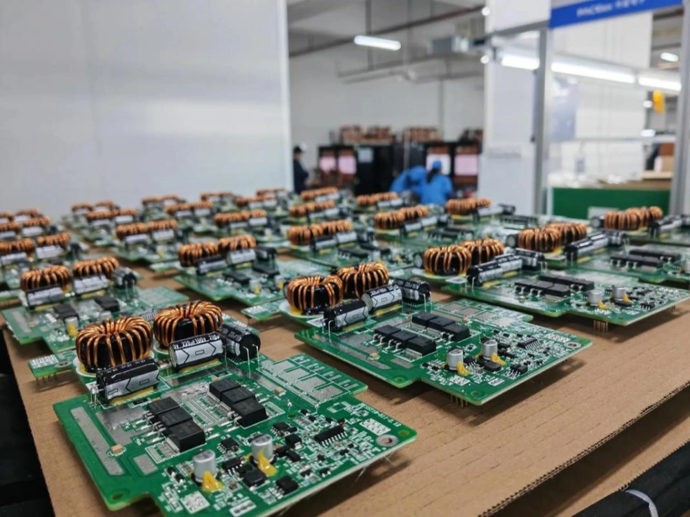
How manufacturing affects BMS reliability
Manufacturing variation matters because BMS circuits often operate near measurement, insulation, and thermal margins. Control plans should connect each important design characteristic to evidence from fabrication and assembly.
| Manufacturing control | Why it matters to a BMS | Useful evidence |
|---|---|---|
| Material and stack-up control | Changes dielectric spacing, impedance, expansion, and thermal behavior | Approved material list, lot traceability, and stack-up record |
| Copper and hole fabrication | Changes current sharing, resistance, inductance, and plated-hole fatigue margin | Cross-sections, coupons, and dimensional inspection |
| Solder-paste and placement control | Affects shunt, MOSFET, AFE, connector, and thermal-pad joints | SPI/AOI data, feeder records, and first-article review |
| Reflow and selective solder control | Affects solder joint formation, component stress, and insulation contamination | Profile records, recipe revision, and solderability evidence |
| Electrical and functional testing | Confirms nets, programming, communications, sensing, and protection behavior | ICT/boundary-scan results, functional test logs, and calibrated equipment records |
| Change control and traceability | Makes a field failure diagnosable and prevents silent substitution | Revision history, deviation approvals, and serialized or lot-based records |
Use a qualification plan appropriate to the product’s environment and risk. Temperature cycling, vibration, humidity, electrical transients, insulation testing, and communication robustness may all be relevant, but the exact tests and limits come from the vehicle, battery, and regulatory requirements. GreatPCB’s PCB testing overview can help organize test categories; it does not define the acceptance limits for a specific BMS.
Automotive standards: keep their scopes separate
Standards are useful only when the team states what each one controls.
| Standard or specification | Relevant scope | What it does not prove by itself |
|---|---|---|
| ISO 26262 | Functional-safety lifecycle, hazard analysis, safety goals, hardware/software development, and verification for road-vehicle E/E systems | That a PCB or supplier is automatically “ISO 26262 compliant” |
| IATF 16949 | Quality-management requirements for automotive production organizations and their processes | That an individual board meets a safety goal or electrical performance requirement |
| AEC-Q100 | Qualification of integrated circuits for automotive use | That the assembled PCB, layout, or BMS system is qualified |
| AEC-Q200 | Qualification of passive components for automotive applications | That a passive component is suitable without checking its actual stress, derating, and application |
| IPC-6012 and related IPC documents | Qualification and performance requirements for specified rigid printed boards; the applicable revision and class matter | Product-level functional safety or vehicle validation |
| IPC-A-600 and IPC-A-610 | Bare-board acceptability and electronic-assembly workmanship, respectively | Cell-monitoring accuracy, EMC immunity, or BMS safety analysis |
| IPC-TM-650 | Test methods used to measure defined board or material properties | A universal pass/fail limit independent of the product specification |
The BMS safety case normally links system requirements to hardware safety mechanisms, diagnostics, fault handling, and verification evidence. Component qualification, factory quality systems, bare-board acceptance, and product-level functional safety are related but not interchangeable.
Common BMS PCB design mistakes
The following mistakes are common because they look acceptable in a schematic or a low-voltage prototype:
- treating “FR-4” or a high Tg as a complete material specification;
- placing the AFE close to the connector but routing its returns through a switching-current region;
- measuring a shunt through shared copper instead of Kelvin connections;
- using one generic clearance value without checking working voltage, transients, pollution, and altitude;
- putting a connector, mounting hole, or test point through the isolation boundary;
- calculating controlled impedance from nominal rather than actual stack-up data;
- allowing balancing heat or MOSFET loss to raise the local temperature of the measurement reference;
- copying an EMC filter from another vehicle without validating harness and enclosure parasitics;
- postponing DFM until after the copper thickness, slots, and package choices are frozen;
- accepting a passing functional test as proof that the board has adequate EMC or environmental margin;
- allowing component substitutions without checking package, dissipation, isolation, timing, and qualification status.
A practical BMS PCB design checklist
Before design release, confirm that the team can answer these questions:
- Which BMS architecture is being used: centralized, modular, or distributed?
- Where are the high-voltage, cell-stack, chassis, and low-voltage domains?
- What are the normal, transient, and fault voltages at every isolation boundary?
- Are creepage and clearance calculated for the actual environment and requirement?
- Are cell-voltage and current-sense routes protected, matched, and Kelvin connected where required?
- Can balancing, contactor, and DC/DC currents return without crossing sensitive analog references?
- Have the worst-case MOSFET, shunt, regulator, and balancing-resistor temperatures been reviewed?
- Is the stack-up based on real dielectric thickness, copper geometry, and material data?
- Are CAN or other communication routes referenced, filtered, terminated, and tested according to the network topology?
- Has the fabricator reviewed heavy copper, vias, isolation slots, panelization, and solder-mask geometry?
- Are SPI, AOI, X-ray, ICT or boundary scan, programming, and functional tests assigned to specific failure modes?
- Are component changes, material lots, firmware revisions, and test records controlled together?
- Does the verification plan cover the vehicle environment rather than only room-temperature bench operation?
FAQ: Automotive BMS PCB design
A BMS PCB is the circuit board that measures cell and pack conditions, controls balancing and protection, processes diagnostics, and communicates with the vehicle or battery controller. Its design may include high-voltage isolation, precision analog measurement, current sensing, MOSFET or contactor control, thermal management, and automotive communications.
There is no single universal BMS PCB type. Automotive BMS products commonly use rigid multilayer boards with copper and dielectric construction selected for the pack voltage, current, temperature, EMC, mechanical, and manufacturing requirements. Centralized, modular, and distributed BMS architectures can use different board sizes, isolation boundaries, and interconnects.
The main challenges are maintaining measurement accuracy next to noisy power switching, routing high current without excessive heat or voltage drop, preserving creepage and clearance across high-voltage boundaries, controlling EMC through the board and harness, and producing the design consistently under automotive quality and traceability requirements.
Start by defining the voltage domains and isolation barriers. Set creepage and clearance from the working voltage, transients, pollution, material, altitude, and applicable requirements. Keep cell-monitoring inputs protected and away from switching loops, use qualified isolation components and power supplies, inspect internal layers and slots, and verify insulation under the product’s defined test plan.
Creepage and clearance reduce the risk of leakage, arcing, and insulation breakdown between battery and low-voltage domains. Clearance is measured through air, while creepage follows the board surface. Required distances are application-specific; a spacing copied from another board is not a valid safety calculation.
Layout affects accuracy through shared voltage drops, magnetic and electric-field coupling, unequal RC settling, ground-reference movement, thermal gradients, and leakage. Short matched routes, Kelvin sensing, controlled returns, local decoupling, protection close to the AFE, and separation from high dV/dt nodes reduce these error sources.
Manufacturing changes can alter copper resistance, via current sharing, dielectric spacing, solder-joint quality, thermal paths, and component identity. Early DFM, controlled material and stack-up records, process monitoring, inspection, electrical testing, and change traceability are needed to connect the released design to the board that enters the vehicle.
No. Tg is only one material parameter. Automotive suitability also depends on z-axis expansion, moisture behavior, copper adhesion, dielectric construction, thermal cycling, insulation requirements, mechanical loading, EMC, component qualification, and the manufacturing process. The complete board and system must be verified against their requirements.
The applicable set depends on the vehicle and customer requirements. ISO 26262 addresses functional-safety development at the vehicle E/E-system level; IATF 16949 addresses automotive quality-management processes; AEC-Q100 and AEC-Q200 qualify ICs and passive components; and IPC documents address board performance, bare-board acceptability, assembly workmanship, and test methods. None of these labels alone proves that a BMS PCB satisfies every system requirement.
Table of Contents
- बीएमएस पीसीबी म्हणजे काय?
- ऑटोमोटिव्ह BMS PCB डिझाइन वेगळे का असते?
- विद्युत डिझाइनमधील विचार
- उच्च-प्रवाह मार्गक्रमण आणि वीज अखंडता
- सरपटणे, साफसफाई आणि विलगीकरण
- ग्राउंडिंग, रिटर्न पाथ आणि सिग्नल अखंडता
- औष्णिक व्यवस्थापन
- ईएमसी आणि ईएमआय नियंत्रण
- घटकांची मांडणी आणि पीसीबी लेआउटचा क्रम
- पीसीबी मटेरियल, स्टॅक-अप आणि तांब्याची जाडी
- उत्पादन आणि जुळवणीसाठी डिझाइन करा
- उत्पादन BMS च्या विश्वसनीयतेवर कसा परिणाम करते
- ऑटोमोटिव्ह मानके: त्यांची व्याप्ती वेगळी ठेवा
- BMS PCB डिझाइनमधील सामान्य चुका
- एक व्यावहारिक बीएमएस पीसीबी डिझाइन चेकलिस्ट
- वारंवार विचारले जाणारे प्रश्न: ऑटोमोटिव्ह बीएमएस पीसीबी डिझाइन
Related Posts
PCBA Prototype
September 8, 2026