Mixed-Signal PCB Design: A Complete Guideline

Introduction
A design review passes with flying colors. The schematics are perfect, and the layout rules are met. Yet, six months later, units start failing in the field—intermittent glitches traced to digital noise corrupting a sensitive analog sensor reading. This silent failure is the hallmark of a board where analog and digital domains collided, not cooperated. Reliable circuits don’t happen by accident; they are the result of strict discipline. Applying proven mixed-signal PCB design guidelines from the initial floorplan to final routing is the only way to prevent a beautiful prototype from becoming a costly field-return statistic. In this guide, we move beyond basic checklists to dissect the physics of return currents and the partitioning strategies that guarantee predictable, low-noise performance.
Understanding Mixed-Signal Fundamentals
To understand analog digital interference, you must first recognize that these two worlds speak fundamentally different languages. An analog signal is continuous—like a microphone’s smooth voltage wave representing sound. A digital signal is discrete—a rapid-fire train of square pulses switching between high and low states to represent ones and zeros. In a mixed-signal PCB, these domains are forced to coexist millimeters apart, and that proximity breeds physics-driven chaos.
The primary mechanism for failure is unwanted coupling. Fast digital switching edges—not just the clock frequency, but the nanosecond rise times—inject high-frequency noise into the shared substrate and power rails. This is where experienced engineers observe ground bounce: a transient voltage spike on the ground reference caused by simultaneous switching noise. If that corrupted ground is shared with a precision analog-to-digital converter, the quantization of your signal collapses.
Furthermore, electromagnetic interference (EMI) radiates from fast loop areas, turning traces into unintentional antennas. Without strict physical partitioning and proper PCB lamination techniques, the return currents from a digital bus can easily couple into a sensitive analog node through fringing fields. The foundation for preventing this lies in a well-designed PCB stackup, where continuous reference planes provide a controlled path for return energy. Recognizing that current flows in loops, not straight lines, is the first step toward a quiet board. This discipline becomes concrete when we translate it into the physical layout, beginning with a rigorous component placement strategy that segregates functional blocks before a single track is routed.
Component Placement and Floorplanning
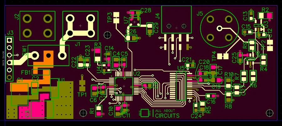
A strategic floorplan does more than organize parts—it physically enforces signal integrity before routing begins. Without this spatial discipline, sensitive analog signals inevitably share return paths with fast digital transients, producing noise that no amount of filtering can fully rescue. The following placement rules, refined through iterative lab validation, isolate these domains from the start.
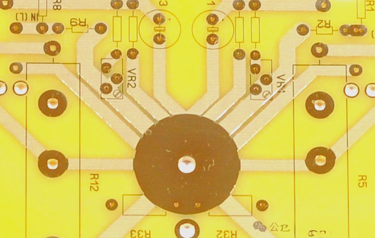
- Segregate by function, then by signal speed. Draw hard boundaries on the board outline separating analog, high-speed digital, and power-conversion blocks. Place the noisiest elements—switching regulators, clock generators, high-current drivers—near the power entry point, farthest from sensitive analog front-ends. This physical distance exploits natural trace inductance to attenuate coupled noise before it reaches precision nodes.
- Anchor the partition around the mixed-signal device. In designs combining ADCs or DACs with microcontrollers, position the converter straddling the analog/digital boundary. This minimizes trace length for both domains and provides a single point where return currents can be managed. Route digital traces away from analog pins immediately, avoiding parallel runs that capacitively couple edge energy into measurement inputs.
- Treat the power supply as a noise source, not a utility. Switch-mode converters generate magnetic fields that radiate into nearby loops. Place them at the board edge and orient inductors so their flux lines point away from high-impedance analog nodes. Follow manufacturer layout examples precisely—deviations from recommended copper geometries often degrade performance by 6–10 dB, a margin easily missed until compliance testing.
- Create isolation moats with passive placements. Use physically large decoupling capacitors and series resistors as barriers between zones. A 1206 ferrite bead or bulk capacitor placed perpendicular to a domain boundary acts as a fence, interrupting high-frequency surface currents that would otherwise spread across the plane. This technique, learned from debugging failed emissions scans, costs nothing in BOM but saves board spins.
- Visualize return currents before committing traces. Every signal leaving a driver must return to its source. At low frequencies, return current spreads across the path of least resistance; above 100 kHz, it follows the path of least inductance directly under the signal trace. Mentally map this loop for every critical net. If a digital return current must flow beneath an analog amplifier to complete its path, the placement is flawed—reshuffle blocks until these loops remain confined within their own zones.
- Lock placement with a design review checklist. Before routing, verify that no high-speed trace crosses a plane split, that analog and digital grounds meet only at a single point under the mixed-signal IC, and that crystal oscillators sit within 10 mm of their clock pins with a solid ground guard ring. This formal checkpoint, adapted from IPC design-for-manufacturing practices, catches layout weaknesses when they cost minutes to fix rather than weeks.
Once this partitioned floorplan is frozen, the stackup and grounding architecture become the next critical decision—topics explored in our PCB stackup design guide. For designs pushing beyond 100 MHz, the placement rules above intersect with transmission-line behavior; our high-speed PCB layout techniques article details those edge cases. If you need a second opinion on a mixed-signal layout, contact our engineering team for a design review.
Grounding and Power Distribution: One Plane or Many?
The debate over grounding in mixed-signal PCB design often feels like a religious war. One camp insists on a unified, solid ground plane; the other swears by splitting analog and digital grounds. The right answer depends entirely on your return current paths.
Unified Ground Plane: The Low-Impedance Approach
A single, continuous ground plane provides the lowest impedance return path for high-frequency signals. Remember, return current flows directly underneath signal traces on the nearest reference plane. A solid plane minimizes loop area, which reduces radiated emissions and susceptibility. For most modern designs with a single mixed-signal IC (like an ADC), splitting the ground plane under the chip creates a slot antenna, often worsening noise. We’ve seen a 10-15 dB improvement in noise floor on a high-speed data acquisition board simply by stitching a previously split plane back together.
Split Ground Planes: The Isolation Tactic
Splitting planes can work for physically isolated circuits with no traces crossing the gap. This technique, often called a moat, prevents noisy digital return currents from flowing through the analog section. However, it requires strict discipline: no signal trace can cross the moat without a bridge. A single missed trace creates a massive return path loop. This approach is common in high-current power electronics where you must contain switching noise, but it’s risky for dense mixed-signal layouts.
Star Grounding: The Low-Frequency Solution
Star grounding connects different circuit grounds at a single physical point. This works well for low-frequency systems (below 1 MHz) where return currents follow the path of least resistance. At higher frequencies, inductance dominates, and return currents follow the path of least impedance—which is the plane directly under the trace, ignoring your star point entirely.
Power Distribution Network (PDN) Decoupling
Your power distribution network strategy must match your grounding scheme. Place decoupling capacitors as close to IC power pins as possible, connecting to the same ground plane the IC references. For mixed-signal parts, follow the manufacturer’s layout guidelines precisely. They often recommend a low-impedance connection between analog and digital ground pins directly under the package.
The Practical Rule
A single solid ground plane with careful component placement—partitioning analog, digital, and high-current sections—outperforms a split plane in 90% of designs. Route digital traces only over the digital section and analog traces only over the analog section. This naturally steers return currents without cutting copper. For the remaining 10%, like extreme isolation requirements, consult the signal integrity fundamentals before reaching for the scissors.
Routing Strategies
After the physical scissors stop cutting, the real discipline begins: routing the traces. This is where mixed-signal routing separates a quiet, high-performance board from one riddled with noise. The goal is simple—keep high-speed switching energy from corrupting sensitive analog measurements. A methodical approach to signal integrity here prevents field failures that no amount of firmware can fix later.
Follow these routing rules to maintain a clean signal path:
- Treat digital traces as aggressors. A fast-rising clock edge acts like a miniature radio transmitter. Route these signals away from analog inputs, and never run them parallel to a sensitive trace over long distances. Crossing at a right angle minimizes crosstalk if paths must intersect.
- Guard sensitive nodes with a shield. Place a quiet, grounded guard trace next to high-impedance analog signals. This intercepts stray electric fields before they couple onto the measurement line. The guard trace must connect to a low-impedance reference, not float.
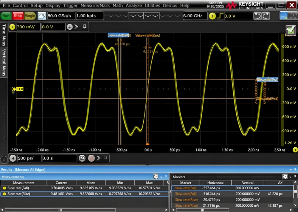
- Lock in differential pair geometry. For high-speed protocols, tight coupling is secondary to matched length. Route the pair side-by-side with constant spacing, and match total length within a few mils. Skew turns a clean differential signal into common-mode noise that radiates.
- Never route over a split reference plane. Return current flows directly underneath the trace on the adjacent reference layer. If that trace crosses a gap between two ground pours, the return path breaks. The resulting loop inductance creates a magnetic antenna and severe signal integrity degradation. Learn more about this fundamental physics in our signal integrity fundamentals guide.
- Bridge plane splits with a stitching capacitor. If a trace must cross from one reference region to another, place a capacitor across the gap to provide a path for high-frequency return current. This is a bandage, not a cure—redesign the stackup if possible.
- Route analog signals on outer layers. Inner layers suffer from via stubs and buried parasitics. Running a sensitive trace on the top layer, directly over an unbroken ground plane, provides the cleanest environment. If you must transition layers, add a ground via next to the signal via.
These practices form the foundation of a robust mixed-signal PCB design workflow. For more detailed spacing requirements, our high-speed routing guidelines provide expanded tolerances for advanced designs.
Stackup Design
The layer arrangement of your PCB—the mixed-signal stackup—is the physical foundation for signal integrity. A poorly planned PCB layer arrangement guarantees coupling between aggressive digital traces and sensitive analog front-ends. The goal is to create a low-inductance, controlled-impedance environment where return currents are predictable.
The table below provides field-proven stackups for 4, 6, and 8-layer boards, assuming standard 1.6mm thickness and FR-4. These configurations prioritize adjacent, uninterrupted ground planes to contain electric fields from high-speed routing and prevent common-impedance coupling.
| Layers | Arrangement (Top to Bottom) | Key Characteristics |
|---|---|---|
| 4-Layer | 1 – Signal (Low-Speed/Digital) 2 – GND Plane 3 – PWR Plane 4 – Signal (Analog) | Best for low-density designs. Never route high-speed signals on this stackup; the lack of an adjacent reference plane for Layer 4 creates high-impedance return paths. |
| 1 – GND Plane 2 – Signal (Analog) 3 – Signal (Digital) 4 – GND Plane | Superior for noise isolation. Burying signals between planes provides 100% shielding. Requires strict PCB layout planning to avoid cutting the planes. | |
| 6-Layer | 1 – Signal (Low-Speed) 2 – GND Plane 3 – Signal (High-Speed Digital) 4 – Signal (Analog) 5 – PWR Plane 6 – Signal (Low-Speed) | Standard high-speed layout. Layer 3 and 4 are tightly coupled to adjacent reference planes. This provides excellent differential impedance control for high-speed interfaces like USB or DDR memory. |
| 8-Layer | 1 – Signal (Analog) 2 – GND Plane 3 – Signal (Digital) 4 – GND Plane 5 – PWR Plane 6 – Signal (Digital) 7 – GND Plane 8 – Signal (Low-Speed) | Maximum isolation for mixed-signal systems. Every signal layer is adjacent to a solid reference plane. Use additional GND planes to physically separate analog and digital routing layers, complementing the component floorplanning strategy. |
For materials, standard FR-4 is lossy above 1 GHz. If your design involves 10+ Gbps serial links or sensitive RF receivers, specify low-loss laminates (e.g., Megtron 6 or Rogers 4350B) on the high-speed layers. Impedance control requires communicating your target dielectric thickness and trace geometry to the fabricator. A tolerance of ±10% is standard; ±5% is achievable for critical 50Ω or 100Ω differential pairs but will increase PCB fabrication cost factors. Always request a controlled-impedance coupon on the panel to verify the actual results, rather than assuming the dielectric constant from the datasheet. A 10% impedance mismatch can significantly degrade signal integrity in high-speed mixed-signal designs.
From Prototype to Production
Next, partner with a manufacturer that offers true engineering support, not just order processing. A capable PCB manufacturer should provide a detailed DFM review that flags potential field-solver mismatches, copper pour imbalances, and solder mask registration issues before fabrication begins. This proactive review prevents the frustrating scenario where a board passes electrical test but fails in the field due to thermal or noise issues. For complex PCB fabrication projects, we recommend manufacturers with integrated assembly capabilities—when the same engineering team oversees both fabrication and prototype PCB assembly, accountability stays in one place.
Case Study: Applying Mixed-Signal Guidelines in an IoT Sensor Hub
When designing an IoT sensor hub, the physical layout often contradicts textbook theory. Our team recently worked on a wearable environmental monitor that combined a sensitive analog front-end (AFE) for gas detection with a high-speed digital IMU and a BLE microcontroller. The initial prototype failed EMC pre-compliance because digital return currents were coupling into the AFE’s low-noise power rail. Applying strict mixed-signal PCB design guidelines, we re-spun the board with a single, unbroken ground plane and a physical "moat" separating the RF digital section from the analog sensors. The challenge wasn’t just the layout; it was sourcing a fabricator capable of holding tight impedance control on a 4-layer, 0.8mm thin core while maintaining the precision routing needed for the split-plane architecture. Partnering with an experienced PCB manufacturer like GreatPCB allowed us to validate the stack-up through their DFM review before committing to production. Their engineering team flagged a potential acid trap in our isolation gap, recommending a slight mask adjustment that preserved signal integrity without compromising the barrier. This direct collaboration between design and fabrication turned a failing prototype into a passing IoT PCB that transitioned smoothly to volume assembly.
Advanced Insights: Simulation and Testing for First-Pass Success
Before a single board is fabricated, virtual prototypes can expose the hidden physics that schematic capture misses. This is where rigorous PCB design validation moves from best-guess to first-pass success. Pre-layout analysis using 2.5D or 3D electromagnetic solvers allows engineers to characterize critical high-speed interconnects and optimize stackup parameters—trace width, spacing, and dielectric thickness—against target impedance long before routing begins. It answers the “what if” questions that prevent late-stage surprises.
Once the physical layout is roughed in, post-layout verification becomes the definitive gatekeeper. Tools like Cadence Sigrity or Ansys SIwave extract S-parameters from the routed board to simulate actual channel behavior, including reflections, crosstalk, and simultaneous switching noise in the power delivery network. This mixed-signal simulation confirms that sensitive analog front-ends remain isolated from aggressive digital transients. As an PCB manufacturing expert would attest, catching a decoupling deficiency here avoids a costly respin later. The final step is running compliance eye diagrams against standards like DDR5 or PCIe Gen5, generating a quantitative pass/fail verdict. This signal integrity testing workflow, paired with a disciplined PCB design guide, transforms theoretical rules into validated hardware confidence.
Frequently Asked Questions
The issue often isn’t the plane itself, but where return currents flow. High-speed digital return current follows the path of least inductance—directly under the signal trace. If analog traces cross that same zone, the shared return path injects digital noise into the analog section. The fix is strict physical partitioning: keep analog and digital routing over their respective ground regions, as detailed in a structured PCB design guide. For single-plane designs, a physical gap in the copper pour between domains prevents this cross-contamination.
A single solid ground plane often works best if you physically separate noisy and quiet sections on the board. Splitting the plane creates a slot antenna unless you bridge it at exactly one point under a single connecting component. If you must split, never route traces across the gap. Our PCB manufacturing capabilities support tight impedance control for both approaches, but the routing discipline matters more than the plane geometry.
Start with a 4-layer baseline:
- Layer 1: Critical analog signals
- Layer 2: Solid ground reference
- Layer 3: Power planes (split analog/digital)
- Layer 4: Digital signals
This puts every signal layer adjacent to an unbroken reference plane, minimizing loop area. For dense designs, a 6-layer stackup adds dedicated routing layers while preserving continuous references. The rapid PCB prototyping phase lets you validate stackup assumptions before committing to volume.
Distance is your first defense. Place analog and digital blocks in separate board regions with a clear boundary. Within analog sections, guard traces connected to the analog reference can shield high-impedance nodes. Clock lines deserve special care—route them as stripline between reference planes and far from analog inputs. Our PCB assembly team often sees field failures traced to a single clock trace routed too close to a sensor input.
Controlled dielectric spacing and copper weight uniformity directly affect impedance and crosstalk. Specify Class 3 inspection if the design includes precision analog front-ends. During turnkey PCB assembly, thermal profiling prevents delamination that shifts dielectric properties. Even small variations in laminate thickness change the capacitance between planes, altering the very noise behavior you simulated.
Conclusion: Building Reliable Mixed-Signal Systems with Proven Guidelines
Successful mixed-signal design isn’t about isolated tricks—it’s a disciplined, end-to-end workflow. From component floorplanning and controlled impedance routing to continuous return paths and material selection, every choice either preserves or destroys signal integrity. When you treat partitioning boundaries as electromagnetic barriers and rigorously apply these mixed-signal PCB design guidelines, you stop chasing intermittent noise problems and start building predictable performance. These system-level habits separate a lab prototype from a reliable field-ready product. For deeper implementation details, explore our guide on high-speed layout techniques or review the fundamentals of power integrity simulation. If you need to validate your specific stackup, our signal integrity consulting services can help identify risks before fabrication.
Ready to Bring Your Mixed-Signal Design to Life?
Whether you are troubleshooting a complex mixed-signal layout or scaling from a working prototype, the right manufacturing partner makes the difference between a design that works on paper and one that performs reliably in the field. Our engineering team provides a free DFM review before production starts, catching potential issues like acid traps, slivers, or insufficient annular rings that can derail a sensitive analog front-end. We don’t just build boards; we help you optimize them for yield. From sourcing long-lead-time components for your BOM to executing a precise SMT assembly process on our automated lines, GreatPCB delivers a fully tested, turnkey solution. One recent medical device client reduced their first-pass failure rate by 15% after implementing our pre-production stackup recommendations. If you need a single prototype or are ready to transition to mass production, today and get a detailed manufacturing review within hours.
Table of Contents

Tags
Related Posts

PCBA Prototype
July 21, 2026
PCBA Prototype
July 17, 2026