
6 Layer vs 8 Layer PCB: Which Is Better for Signal Integrity?
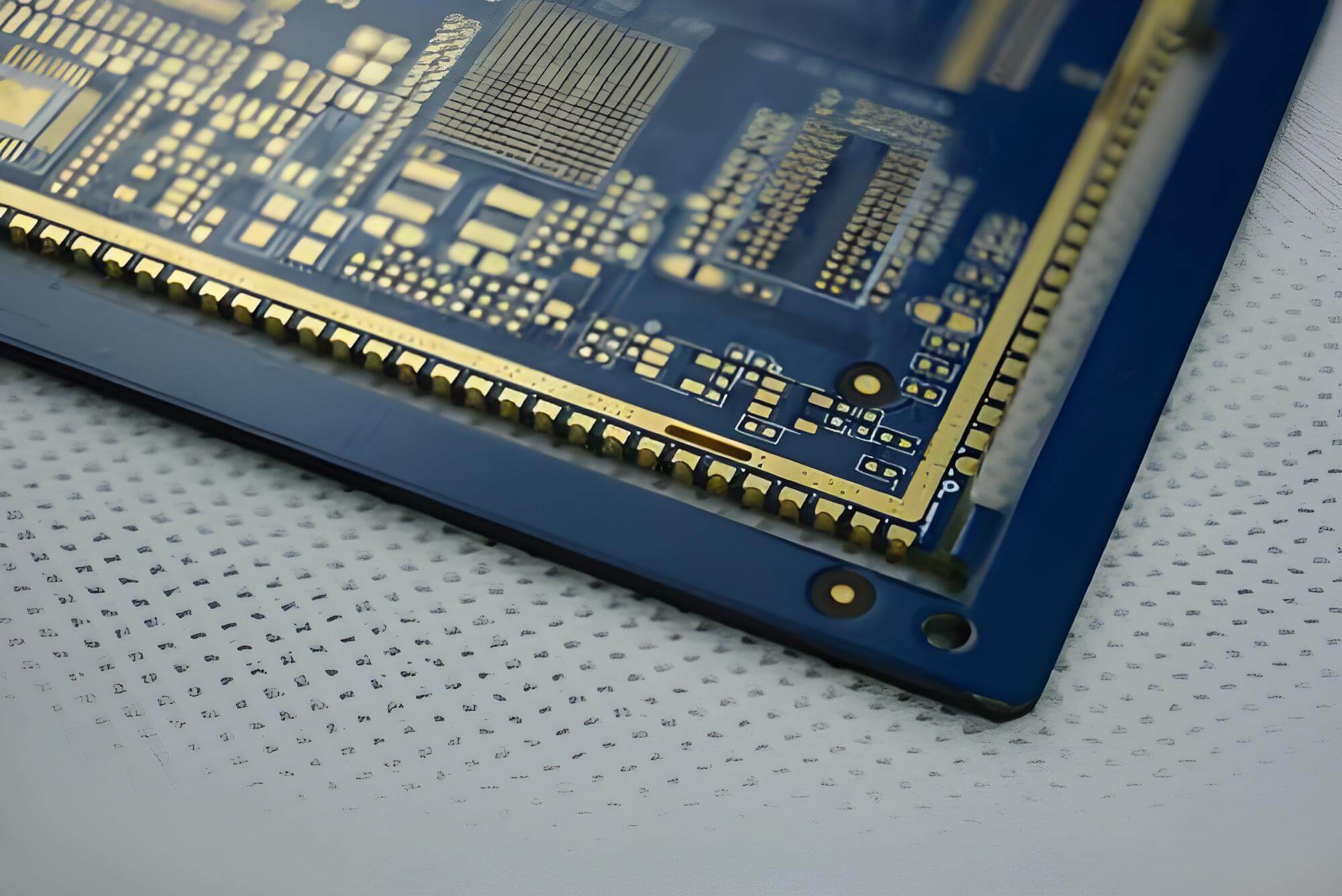
Choosing between a 6-layer and an 8-layer PCB stackup is rarely about the dollar figure on the fabrication quote. It’s about whether your high-speed signals have a reliable return path and whether your design can survive the rigors of volume PCBA assembly without degradation. If you’re seeing intermittent EMI failures or marginal eye diagrams on a 6-layer prototype, adding two more layers might help—but only if you use them correctly.
The 6-Layer Benchmark and Where It Falls Apart
Most engineering teams default to 6 layers because it’s the minimum that allows separate planes for power and ground while still offering four routing layers. The classic stackup—Signal, Ground, Power, Signal, Ground, Signal—works well at moderate speeds if you keep critical traces on layers adjacent to unbroken planes. The moment you route a DDR4 clock across a split plane or transition a USB 3.0 differential pair between non-adjacent references, it stops working.
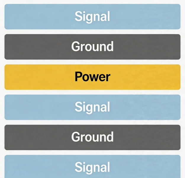
The problem isn’t the layer count. It’s the return path discontinuity.
On a 6-layer board, you’re often forced into asymmetric stackups: two signal layers share a power/ground cavity, while a third signal layer sits opposite a ground plane. The moment a high-speed signal leaves the well-referenced region and jumps to a layer that references a split power plane, the return current spreads across stitching capacitors and vias. You get common-mode noise, crosstalk, and emission problems that no amount of series termination can fix.
I’ve seen a design team spend three weeks debugging an intermittent Ethernet PHY failure that disappeared when they re-spun the board as an 8-layer with a proper symmetrical stackup. The root cause wasn’t the PHY or the layout—it was the return path gap on Layer 5 that the 6-layer stack couldn’t close without sacrificing another signal’s routing channel.
Why Most 8-Layer Designs Succeed—Based on Planes, Not Vias
Adding two more layers changes the game only when you allocate them to planes, not to more signal routing. The winning 8-layer configuration is usually symmetrical (such as Signal, Ground, Signal, Power, Ground, Signal, Ground, Signal) to ensure tight power-ground cavity coupling. This arrangement lets every high-speed signal layer sit adjacent to an unbroken reference plane, and it eliminates split-plane crossings for almost all aggressive interfaces.
The benefit manifests in three specific ways:
Predictable Impedance Control: You can route 100-ohm differential pairs on Outer layers, 90-ohm pairs on internal layers, and still hit $\pm8\%$ tolerance without heroic dielectric control. On a 6-layer board, getting those same margins often requires thinner prepregs that push the fabricator into tighter process windows—and those windows cost yield.
Improved Power Integrity (PI): You can dedicate an entire layer pair to a low-inductance power-ground cavity. That matters when you’re sequencing multiple supply rails with sub-10 mV ripple targets.
Reduced Crosstalk: When a high-speed aggressor can’t couple edge-to-edge onto another signal layer three prepregs away, the near-end crosstalk coefficient falls below $-40\text{ dB}$ without guard traces. That lets you route denser parallel buses without adding spacing.
None of this works if you take an 8-layer stackup and fill the extra layers with noisy routing. I’ve reviewed boards where someone added two layers and proceeded to route 1.2 GHz clocks adjacent to sensitive analog traces on the same internal cavity, effectively wasting the two layers they paid for. More layers don’t fix poor assignment discipline.
Stackup Comparison for Critical Signals
| Parameter | Typical 6-Layer (Asymmetric) | Optimized 8-Layer (Symmetric) |
| Signal layers with solid reference | 3 out of 4 (often one compromised) | All signal layers adjacent to unbroken plane |
| Impedance tolerance (differential) | $\pm12\%$ typical without special materials | $\pm8\%$ repeatable with standard FR4 |
| Power plane inductance | Shared cavity, moderate | Dedicated cavity, low inductance |
| Crosstalk between adjacent signal layers | Can be problematic if poorly stacked | Nearly eliminated by plane separation |
| Routing flexibility for BGA escape | Tight; often forces extra layers for full breakout | Comfortable for 0.8mm pitch and denser |
The Assembly Equation—How Layer Count Influences PCBA Yield
The discussion usually stops at signal integrity. That’s a mistake. Layer count shifts PCB fabrication properties that feed directly into PCBA assembly reliability, and engineers who ignore this step see yield drops they can’t explain.
An 8-layer board, especially one with a symmetric stack, tends to be mechanically more stable during reflow. The balanced copper distribution and symmetric dielectric layers reduce warpage at soldering temperatures. On a 6-layer board, if the stackup is asymmetric, the board can bow during the reflow profile, lifting fine-pitch BGA corner balls just enough to create Head-in-Pillow (HiP) defects that pass initial electrical test but fail after the first few thermal cycles in the field.
In an automated SMT line running 24/7 with placement accuracy of $\pm0.03\text{ mm}$, that slight planarity variation doesn’t stop the pick-and-place from placing the part accurately. It affects the reflow wetting dynamics in ways that AOI sometimes misses. I’ve field-returned assemblies where cross-section analysis revealed BGA joints that looked perfect on X-ray but had a hairline crack at the package-to-board interface—the hallmark of warpage-driven failure that a 6-layer asymmetric stack promoted.

During DFM review, which should always include signal integrity, power integrity, and EMC evaluation, I specifically ask the fab house to simulate the reflow bow and twist for any board crossing 1.6 mm total thickness or having more than two types of prepreg. Balanced 8-layer builds naturally achieve symmetry with matched glass styles (like avoiding mixing 106 and 2116 prepregs asymmetrically).
Assembly also demands impedance predictability after lamination. The more layers you have, the more critical it becomes that the fabricator’s oxide treatment creates consistent roughness without eating into trace width. A 2-mil trace on Layer 1 of an 8-layer PCB needs to come out at 2 mil after surface preparation, not 1.8 mil because of an aggressive oxide cycle. That small dimension loss shifts the impedance enough to misalign your termination assumptions, showing up as marginal jitter during functional test—the most expensive place to find it.
When Six Layers Still Makes Sense
Don’t interpret the above as a blanket recommendation for 8 layers. Circumstances exist where 6 layers outperform an 8-layer design—not in raw SI margins, but in overall project success.
If your fastest signal runs at 100 MHz and you’re not pushing DDR4 or high-speed serial lanes, you don’t need the extra plane isolation. A well-designed 6-layer board with contiguous ground on layers 2 and 5 and careful routing discipline can easily pass radiated emissions and maintain adequate timing margins. The cost of those two extra layers—roughly 20–30% more in fabrication at medium volumes—buys zero additional value in such a design.
Also consider thickness constraints. An 8-layer board often ends up thicker than a 6-layer board unless you force thinner dielectrics that drive up material cost and reduce manufacturing yield. If the enclosure only accepts a 1.0 mm board, forcing eight layers into that envelope means resorting to thin prepregs and HDI microvias, which raises the cost disproportionately.
The decision isn’t about layer count; it’s about whether you can maintain an unambiguous return path for every critical signal. When the PCB designer understands the difference between a plane and a reference, six layers can go further than many engineers expect.
What a DFM Review Reveals Before Tape-Out
By the time you’re debating 6 versus 8 layers, you should already have run a pre-DFM check. Not the automated software check—an actual review that includes a fabricator or assembly partner who can look at your specific stackup and production volume. Every quotation from a competent manufacturer should include a detailed design-for-manufacturing evaluation at no extra cost.
That review will answer questions you didn’t know to ask:
Will the fabricator’s lamination press handle your proposed dielectric thicknesses without resin starvation on the inner layers?
Does the board thickness push you into a different drilling parameter set that increases hole-wall roughness and degrades plated-through-hole reliability?
On an 8-layer board where you’re relying on laser-drilled microvias down to 4 mil, are those vias staggered or stacked, and does the fab have the registration capability to stack them with less than 25 μm misalignment?
These questions matter because process capability directly translates into signal integrity after assembly. A via that is plated slightly thinner than nominal introduces a small impedance bump. On a 6.25 Gbps differential pair, one such bump may be tolerable. On a 10 Gbps+ link, it closes the eye. The 8-layer board you selected for signal integrity ends up failing acceptance test—not because the design was wrong, but because the fab couldn’t maintain the via geometry across the whole panel.
The Real Takeaway
Engineers often treat layer count as a binary choice driven by electrical simulation. It’s not. It’s a system-level trade-off that touches signal return path quality, power delivery impedance, assembly warpage, fabrication capability, and testing cost.
Before finalizing your layer count, verify that your stackup works not just in simulation, but within your fabricator’s real process window and your assembly partner’s proven capability. A few hours of up-front DFM review that pairs SI requirements with manufacturing reality will save more signal integrity than any arbitrary increase in layer count ever could.
After choosing the layer count, confirm the PCB stack-up design and controlled impedance requirements before fabrication.
For broader Multilayer PCB guidance, see Multilayer PCB overview.
Table of Contents
- 6 давхаргын жишиг үзүүлэлт ба түүний нуралт
- Яагаад ихэнх 8 давхаргат загварууд амжилттай байдаг вэ? - Виас биш, хавтгай дээр суурилдаг
- Чухал дохионуудын stackup харьцуулалт
- Ассемблерийн тэгшитгэл - Давхаргын тоо нь PCBA гарцад хэрхэн нөлөөлдөг вэ
- Зургаан давхарга утга учиртай хэвээр байх үед
- DFM-ийн тойм нь Tape-Out-оос өмнө юуг илчилдэг вэ
- Жинхэнэ дүгнэлт
Related Posts
PCBA Prototype
September 8, 2026