Automotive Radar PCB Design: Materials, Stackup and SI
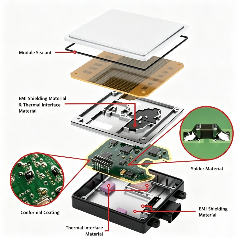
An automotive radar PCB is the circuit board that supports the radar RF path, antenna interface, radar IC, clocking, power distribution, digital processing, and vehicle communications. Its job is not simply to connect components. It must preserve predictable RF behavior while surviving the thermal, mechanical, manufacturing, and quality demands of an automotive program.
Automotive radar PCB design is different from general automotive PCB design because RF performance is part of the product function. It is also different from a general high-frequency PCB because the board must be repeatable at production scale and evaluated against the vehicle program's environmental and quality requirements. The design chain is direct:
Radar frequency affects material and transmission-line choices; material and stackup determine impedance and loss; routing and vias introduce discontinuities; those choices affect DFM, test strategy, and long-term reliability.
What frequencies do automotive radar PCBs support?
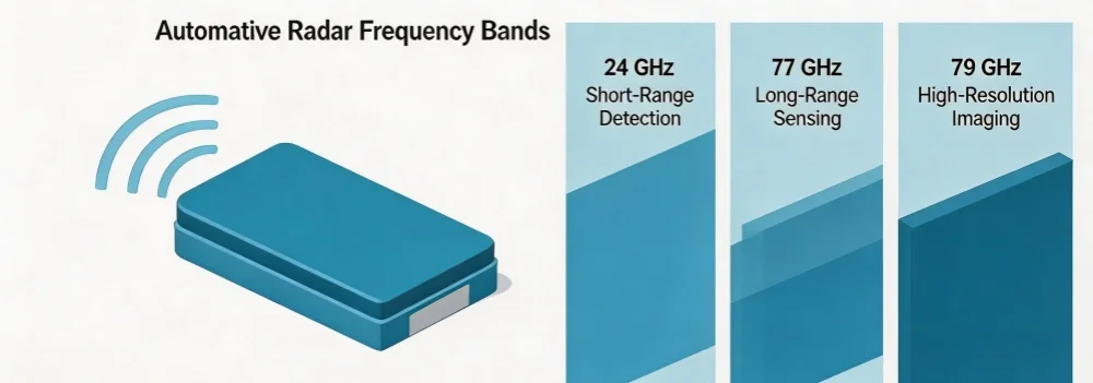
Automotive radar implementations are application- and market-dependent. The labels 24 GHz, 77 GHz, and 79 GHz describe operating bands or product terminology, not three universal PCB construction recipes.
| Radar context | PCB design consequence | Practical caution |
|---|---|---|
| 24 GHz radar | RF loss, return paths, antenna integration, and impedance still matter, but the longer wavelength generally makes a given layout feature electrically less severe than at mmWave frequencies. | Do not treat 24 GHz as automatic permission to use any FR-4 stackup. Validate the actual path length, loss budget, antenna architecture, and temperature behavior. |
| 76-81 GHz radar | This mmWave range is common in current automotive radar IC platforms. Small changes in trace geometry, dielectric behavior, copper surface profile, launches, and assembly can become material to performance. | "77 GHz" and "79 GHz" products may have different system needs, but they do not imply fixed layer counts or a single mandatory laminate family. |
| Short-, medium-, and long-range ADAS radar | Field of view, antenna arrangement, transmit/receive channel count, package, thermal load, radome, and packaging constraints can all change the board design. | Range category is a system requirement. It should not be inferred from a PCB material alone. |
For example, TI's AWR2944 is an automotive radar SoC specified for 76-81 GHz operation. That is useful evidence of a current commercial band, but it is not a fabrication specification for every 76-81 GHz board. Regional radio requirements also apply at the product level. In Europe, ETSI EN 302 264 addresses radar equipment in the 77-81 GHz band; the applicable regulation and approval path must be confirmed for each target market.
Why does radar frequency change PCB design requirements?
Higher frequency shortens wavelength and reduces tolerance for unintended electrical length, parasitic capacitance, parasitic inductance, and dielectric loss. A trace that is electrically modest at lower frequency can become a meaningful transmission line at 77-81 GHz. A via, pad transition, solder-mask boundary, plane void, or copper texture can then alter insertion loss, return loss, phase, or coupling.
Frequency does not act alone. The critical inputs are the operating band, RF path length, antenna topology, allowable loss and phase error, board geometry, temperature range, and production variation. The correct question is not "What material is used for 77 GHz?" It is "Which material system and stackup meet this radar's electrical and manufacturing requirements with margin?"
Why is PCB material important for automotive radar?
PCB material affects radar performance through dielectric constant, dielectric loss, thickness control, resin and glass construction, thermal behavior, copper interface, and fabrication consistency.
- Dielectric constant (Dk) affects propagation velocity and the geometry needed to achieve a target impedance. Dk variation can change electrical length and phase relationship.
- Dissipation factor (Df), often called loss tangent, contributes to dielectric attenuation. Its importance rises as frequency and routed RF length increase.
- Thermal and mechanical behavior affects registration, plated-through-hole reliability, warpage, and the stability of geometry through manufacturing and use.
- Copper roughness adds conductor loss at high frequency because current is concentrated near the conductor surface. The relevant value is the copper treatment and profile in the released material system, not a generic statement that a laminate is "low loss."
Material data must be read with its test method, frequency, construction, copper treatment, and processing assumptions. A nominal Dk from a data sheet is not enough to release a production impedance table. The fabricator should calculate the stackup using the actual core, prepreg, copper, plating, and finished dielectric conditions.
When is standard FR-4 suitable for automotive radar?
A characterized FR-4 construction can be suitable for portions of an automotive radar PCB when the RF loss and phase budget permit it. Examples can include power, digital, control, and short RF sections in a validated architecture. It can also be part of a hybrid construction where the most loss-sensitive RF path uses a different material.
FR-4 is not suitable or unsuitable solely because a design is called "radar." At 24 GHz, a well-characterized FR-4 construction may be feasible for some architectures. At 76-81 GHz, longer or more loss-sensitive RF paths often justify a lower-loss material system, but the decision still depends on the design budget and validation data.
When should Rogers or other low-loss materials be considered?
Consider a low-loss RF laminate when the loss, phase stability, Dk control, antenna efficiency, or temperature behavior of the actual RF path cannot be met with the proposed FR-4 construction. This can be especially relevant for 77 GHz and 79 GHz radar paths, antenna feed networks, and other electrically long mmWave structures.
Rogers is a manufacturer and product family, not a generic technical requirement. Its RF laminate portfolio includes material families with different electrical, thermal, and processing characteristics. PTFE-family, hydrocarbon-ceramic, and low-loss thermoset materials also have different assembly, drilling, registration, bonding, and supply-chain trade-offs. The material selection must be made at the qualified stackup level, not by brand name alone. For broader background, see GreatPCB's guide to Rogers PCB materials.
| Selection factor | Why it matters to radar | Design decision |
|---|---|---|
| Dk and Dk consistency | Controls impedance, electrical length, and phase repeatability. | Use supplier data for the intended construction and let the fabricator model the finished stackup. |
| Df and conductor loss | Reduces RF energy reaching the antenna or receiver as frequency and path length rise. | Compare total channel loss, not Df in isolation. |
| Thermal behavior | Temperature changes can affect material dimensions and electrical response. | Review the vehicle-zone temperature profile and the complete material system. |
| Manufacturability | Drill quality, lamination flow, plating, registration, and yield affect RF geometry. | Select materials the intended fabricator can build and control repeatedly. |
| Cost and availability | Specialty laminates and compatible prepregs can affect lead time and program cost. | Qualify realistic sources and avoid an electrical choice that cannot be supplied at volume. |
How does stackup affect automotive radar performance?
An automotive radar PCB stackup defines the dielectric spacing, reference planes, trace geometry, isolation strategy, and layer-to-layer transitions. It is therefore an electrical design artifact, not a mechanical afterthought.
A practical stackup separates the functions that need predictable RF behavior from the functions that create noise or heat. A common design direction is to place sensitive RF transmission lines next to a continuous reference plane, keep antenna feeds and RF transitions short, provide controlled return paths, and use internal layers for power and digital routing where appropriate. The exact layer count, RF layer position, and material distribution depend on the antenna and package architecture.
The stackup should be frozen before critical RF routing is released. If dielectric thickness, copper weight, prepreg flow, or reference-plane geometry changes after the impedance calculation, the trace width and electrical performance can change. GreatPCB's PCB stack-up overview is a useful starting point for the fabrication conversation.
Transmission-line geometry: microstrip, stripline, and differential structures
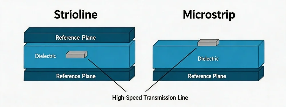
Microstrip and stripline are common controlled-impedance structures, but neither is universally better for radar.
- Microstrip can be useful where an outer-layer RF path or antenna feed is required. Its fields are partly in air and partly in dielectric, so solder mask, nearby metal, and surface conditions require attention.
- Stripline can provide stronger field containment and isolation inside the board, but it has fabrication and transition trade-offs and may have different loss behavior.
- Differential routing is relevant where the radar IC, clock, high-speed digital interface, or a balanced RF structure requires it. It should not be assumed that every RF trace is a differential pair.
Use field-solver results for the released construction, then verify the result with controlled coupons or other agreed fabrication evidence. For the underlying design concept, see controlled impedance PCB design.
Why is controlled impedance important for radar PCBs?
Controlled impedance keeps the transmission-line impedance close to the value expected by the radar IC, matching network, filter, antenna feed, or other RF block. A mismatch can cause reflection, additional loss, amplitude error, phase error, or degraded repeatability.
At radar frequencies, impedance control is a system of variables: trace width, copper thickness, dielectric height, Dk, reference plane, solder-mask condition, etch compensation, plating, launch geometry, and fabrication tolerance. Specifying only a target such as "50 ohm" is incomplete. The drawing or fabrication package should identify the relevant layers, reference planes, target impedance, tolerance where justified, coupon needs, and the stackup revision used for the calculation.
How do routing and vias affect RF signal integrity?
Routing and vias affect radar PCB performance because every discontinuity changes the electromagnetic field. The impact increases when a transition is electrically large relative to wavelength or when it interrupts a return path.
Keep RF paths short, intentional, and phase-aware
Route RF paths only as long as their function requires. For phase-sensitive paths, match electrical length, not just visible trace length. Pads, bends, layer changes, vias, and component launches contribute electrical length and parasitics. Channel matching should be based on the radar architecture, simulation, and device guidance rather than a blanket length-matching rule.
Avoid arbitrary 90-degree corners, neck-downs, isolated copper islands, and unexplained reference-plane changes in sensitive RF paths. Curved or mitered routing is not a substitute for an impedance- and transition-aware layout.
Design via transitions as RF structures
A signal via can add inductance, capacitance, stub resonance, and mode conversion. A high-frequency automotive PCB should minimize unnecessary RF layer changes and use a deliberate transition strategy where a layer change is unavoidable. Depending on the design and fabricator capability, that can include short transitions, nearby ground-return vias, controlled antipads, blind or buried vias, or back-drilled stubs.
None of those techniques should be added by template. They affect cost, yield, and reliability. The correct via structure is the one validated for the board's band, stackup, launch, and production process.
Protect return paths, isolation, and the RF front end
Every RF trace needs a defined return-current path. Do not route a sensitive RF line over a split reference plane, uncontrolled void, or changing reference without analyzing the return transition. Use ground fencing, shielding partitions, keep-outs, and physical separation only where they support a measured or simulated isolation need; poorly positioned ground features can also perturb the intended field geometry.
Place the RF front end, antenna feed, matching networks, reference clock, switching power supplies, and high-speed digital interfaces with coupling paths in mind. The PCB cannot improve an IC's intrinsic phase noise, but poor clock return paths, power-distribution resonance, or switch-node coupling can add spurs and noise that make the radar system harder to validate.
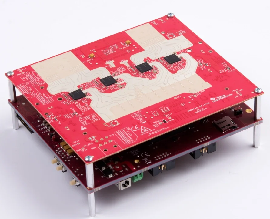
Thermal, environmental, and mechanical reliability requirements
Automotive radar hardware must be designed for the environment in which it is installed, not a generic temperature statement. Enclosure location, self-heating, solar loading, airflow, vibration, moisture, contamination, and assembly mass all affect the actual design margin.
Use copper planes, thermal vias, component placement, interface materials, and enclosure paths to move heat without compromising the RF reference structure or antenna region. Thermal vias near a hot component can be appropriate, but their placement must be evaluated around RF structures and ground returns.
The ISO 16750 series provides road-vehicle environmental-conditions and testing guidance for electrical and electronic equipment; the design team must identify the applicable part or parts for the program. It does not certify a PCB by itself. Likewise, an AEC-Q100-qualified radar IC is an IC qualification statement, not proof that the completed PCB or PCBA meets a vehicle program's requirements. The design owner, component suppliers, and manufacturing partner need an agreed qualification plan for the intended vehicle zone and customer requirements.
Mechanical details also matter. Connector mass, board restraint, mounting-hole placement, panel break-off features, heavy components, and CTE mismatch can change vibration response and solder-joint reliability. If conformal coating or potting is considered, evaluate its dielectric effect near exposed RF lines, antennas, and tuned structures before treating it as a universal reliability improvement.
DFM and PCB fabrication for automotive radar
Radar DFM begins while the stackup and RF geometry are still changeable. A fabricator needs more than Gerbers to evaluate a high-frequency automotive board responsibly. Provide the material callout, stackup, impedance targets, copper requirements, controlled features, finished thickness, hole and via structures, surface-finish constraints, panelization limits, and the test or coupon expectations.
The design review should examine:
- Whether the specified material system, prepregs, and copper treatments are available and compatible.
- Whether finished dielectric thickness, etch compensation, plating, and registration can hold the intended RF geometry.
- Whether RF vias, back drilling, aspect ratios, and annular-ring requirements are buildable at the target volume.
- Whether the surface finish and solder-mask definition support the RF, assembly, corrosion, and inspection needs.
- Whether the panel, fiducials, tooling, and component keep-outs support placement accuracy and mechanical reliability.
The applicable board performance specification and customer acceptance criteria should be identified contractually. Standards such as IPC rigid-board specifications can inform workmanship and performance expectations, but they do not replace radar-specific electrical validation.
GreatPCB supports automotive radar PCB manufacturing, high-frequency materials, and assembly with early DFM engagement.
PCBA, RF testing, and production verification
PCB fabrication control is necessary but not sufficient. Assembly can alter RF performance through component placement, solder volume, package coplanarity, voiding, connector launches, contamination, and rework history. A radar PCBA plan should therefore connect board-level control to the system-level RF verification that the design requires.
| Verification layer | What it can establish | What it cannot establish alone |
|---|---|---|
| Material and fabrication records | The intended construction and controlled features were built as specified. | Final radar range, object classification, or vehicle-level compliance. |
| Impedance coupon or agreed electrical coupon | Whether a defined transmission-line structure tracks the released fabrication target. | The behavior of every antenna, package launch, or complete RF channel. |
| AOI, X-ray, and solder-joint inspection where applicable | Assembly defects, hidden-joint evidence, and placement quality. | RF sensitivity or antenna-pattern performance by themselves. |
| Board and system RF test | Gain, loss, matching, calibration, chirp integrity, channel balance, or other agreed measurements. | A substitute for environmental and vehicle-level validation. |
The test plan should specify what is measured, at which stage, with which fixtures, limits, sampling plan, correlation method, and disposition process. GreatPCB's PCB test page can help frame a conversation about manufacturing and inspection options, but the radar design owner must define the RF acceptance criteria and system test method.
Automotive radar PCB design checklist
Use this checklist before releasing a radar PCB for prototype or production review.
- State the operating band, target market, radar architecture, channel count, and antenna approach.
- Define the RF loss, phase, impedance, thermal, and reliability budgets before selecting material.
- Select the complete material system, including cores, prepregs, copper treatment, and compatible processing materials.
- Freeze the controlled stackup before finalizing critical RF widths and spacings.
- Calculate impedance from the actual fabricator stackup and specify coupon or verification requirements where needed.
- Review microstrip, stripline, differential, and antenna-feed structures against their intended reference planes and surroundings.
- Match phase-sensitive paths electrically, including pads, vias, launches, and layer transitions.
- Minimize RF discontinuities; document any necessary via transition and ground-return strategy.
- Separate RF-sensitive regions from switch nodes, noisy power paths, clocks, digital interfaces, and mechanically disruptive features.
- Review thermal paths, vibration constraints, moisture exposure, and any coating or potting effect near RF structures.
- Confirm DFM, material availability, panelization, assembly access, inspection, and rework constraints with the manufacturing partner.
- Define fabrication, assembly, RF, environmental, and system-level verification as separate but connected activities.
FAQ: automotive radar PCB design
An automotive radar PCB carries and controls the radar system's RF, antenna, clock, power, digital, and vehicle-interface circuitry. It is designed so that the intended electromagnetic behavior can be manufactured and maintained in an automotive environment.
At 77-81 GHz, small layout, material, copper, and transition changes can become electrically significant. The challenge is not a single frequency label; it is achieving the required loss, matching, phase, isolation, and repeatability in the released stackup and production process.
FR-4 can be suitable when the validated RF loss, phase, temperature, and manufacturing budget permit it. It is often used for non-RF sections and can be viable in selected RF architectures. Its suitability must be demonstrated for the actual stackup and channel, not assumed from frequency alone.
Consider a low-loss material when the required mmWave path loss, phase stability, Dk control, antenna performance, or thermal behavior cannot be met with the proposed FR-4 construction. The decision should compare a qualified material system, fabrication capability, cost, and availability, not a brand name alone.
Stackup sets the dielectric height, reference planes, transmission-line geometry, layer transitions, and isolation conditions. Those inputs determine impedance, electrical length, loss, coupling, and the practical limits of the fabrication process.
Controlled impedance reduces mismatch between transmission lines and RF circuit blocks. This helps preserve matching and repeatability. It requires an agreed stackup and geometry, not merely an impedance value written on a drawing.
Vias, pads, bends, plane changes, and stubs can create discontinuities that add reflection, loss, coupling, or phase error. Short, intentional paths with defined reference and return transitions are more reliable than generic high-frequency routing rules.
Common challenges include material availability, dielectric-thickness control, copper treatment, etch compensation, registration, RF via construction, panel stability, placement accuracy, and validating that the released RF geometry is repeatable at production volume.
Testing is layered. Fabrication evidence and impedance coupons can verify controlled board features; assembly inspection can find placement and solder defects; RF and system tests verify the radar behaviors defined by the design owner. No single PCB test proves complete vehicle radar performance.
From radar design intent to manufacturable hardware
The most effective automotive radar PCB programs bring the PCB manufacturer and assembler into the design review before critical material, stackup, via, and test decisions are fixed. GreatPCB can support an early manufacturing discussion for automotive PCB manufacturing and assembly and high-frequency PCB requirements. Bring the released stackup, RF constraints, design files, and validation plan so the discussion can focus on buildable, evidence-based choices.
GreatPCB supports automotive radar PCB manufacturing, high-frequency materials, and assembly with early DFM engagement.
Table of Contents
Related Posts
PCBA Prototype
October 23, 2026
PCBA Prototype
October 19, 2026