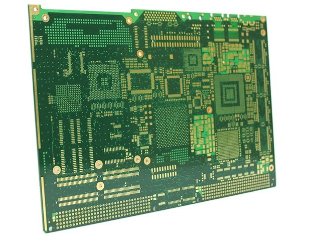
Why Does PCB Delamination Happen? Causes and Prevention
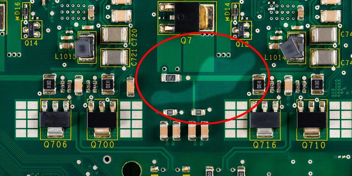
PCB delamination happens when bonded layers inside a printed circuit board lose adhesion or separate under heat, moisture, mechanical stress, or a combination of these factors. The failure can occur between copper and dielectric, between a core and prepreg, within the resin system, or around a plated hole. Moisture trapped in the laminate is a common trigger during lamination or reflow, but the root cause is usually a combination of material selection, board construction, process control, and handling.
Delamination matters because a board can pass an initial electrical test and still contain a growing internal separation. The defect can change impedance, weaken the board, create paths for moisture or contamination, reduce insulation margin, or contribute to later interconnect failure. A raised blister is obvious; an internal interface failure may require microsectioning or acoustic inspection to find.
Quick answer: Prevent PCB delamination by selecting a laminate and stack-up with adequate thermal and mechanical margin, controlling moisture before lamination and assembly, qualifying the lamination process, using a profile appropriate for the actual board and material, and verifying the result with visual inspection plus cross-section or other suitable testing. A delaminated multilayer board is not normally restored to its original reliability by simple adhesive repair.
What is PCB delamination?
PCB delamination, also called PCB laminate delamination, is the unwanted separation of layers that should remain bonded in a laminate structure. A multilayer PCB is built from copper foils, cured cores, and prepreg. During lamination, heat and pressure make the resin flow, wet the adjacent surfaces, fill the intended geometry, and cure into an insulating bond. Delamination occurs when that bond fails or when internal vapor pressure and thermal strain exceed the local strength of the structure.
The word is sometimes used loosely for several different defects. For diagnosis, identify the actual interface and failure mode instead of treating every pale mark or bubble as delamination.
| Condition | What it means | Typical evidence |
|---|---|---|
| Delamination | Separation at an interface or within the laminate, often producing a gap or lifted layer | Cross-section, scanning acoustic microscopy, visible blister, edge lift, or electrical/mechanical change |
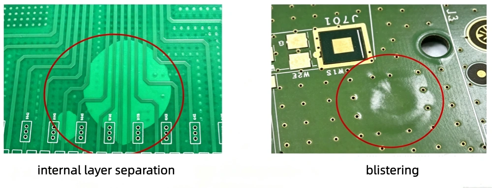
| Blistering | A local bulge caused by a separated region or trapped gas; it is a visible symptom, not a complete root-cause description | Raised surface, bubble, or localized swelling |
| Measling | Small light spots caused by local resin/glass cracking or separation around glass bundles; limited measling is not automatically the same as a continuous interlayer delamination | White crosses or spots under light, sometimes after thermal stress |
| Crazing | A network of resin/glass microcracks or local structural separation, often visible as whitening | Magnified visual inspection or microsection |
| Barrel cracking | A crack through the plated-through-hole copper barrel, often driven by z-axis expansion and thermal cycling; nearby dielectric damage should be recorded separately | Microsection, electrical intermittence, or thermal-stress testing |
| Pad or foil lift | Copper separates from the laminate at a pad or foil interface | Visual inspection, pull testing, microsection, or continuity change |
Measling can be a workmanship or reliability concern depending on its extent, location, product class, and governing acceptance criteria. It should not be used as a shortcut diagnosis for every white spot. The applicable board specification and product class should define the acceptance decision; the IPC standards catalog is the place to confirm the relevant document and revision.
Why does PCB delamination happen?
The main PCB delamination causes are moisture-driven vapor pressure, thermal expansion mismatch, weak or contaminated lamination interfaces, fabrication damage, and mechanical or thermal loading beyond the board’s qualified margin. The physical mechanism is usually a stress imbalance. The laminate absorbs moisture, expands when heated, and changes stiffness as the resin approaches and passes its glass-transition region. Copper, glass reinforcement, resin, and plated holes do not expand equally in every direction. If the interface is weak, contaminated, poorly cured, or already damaged, the resulting strain can open an existing gap or extend a crack, allowing the separation to grow.
| Trigger or stage | Physical mechanism | What to verify |
|---|---|---|
| Material and stack-up | Resin, glass, copper, and plated holes expand differently; insufficient thermal or mechanical margin concentrates strain | Laminate datasheet, resin system, Tg, Td, z-axis CTE, copper balance, and approved stack-up |
| Lamination | Incomplete cure, poor wet-out, contamination, trapped air, or insufficient resin fill leaves a weak interface | Press recipe, material lots, vacuum/pressure history, and a cross-section through the suspect layer |
| Drilling and routing | Heat, smear, burrs, microcracks, edge damage, or depanelization stress create a site that can open later | Tool condition, desmear, hole-wall quality, routing/edge inspection, and defect location |
| Storage and reflow | Absorbed moisture can generate vapor pressure during rapid heating while resin softens and z-axis expansion rises | Exposure history, conditioning decision, actual board profile, thermal-pass count, and post-reflow inspection |
This is why a delamination investigation should trace the whole material-to-assembly chain. Finding the first visible blister does not establish whether the initiating defect was moisture, lamination, drilling, or handling.
1. Moisture absorption and rapid heating
Moisture is a major risk because PCB laminate is not perfectly moisture-proof. Water can enter through board edges, exposed glass/resin, drilled holes, handling, or storage in a humid environment. During a rapid heating step, absorbed moisture can generate local vapor pressure faster than it can diffuse out of the board. The pressure is most damaging where the resin bond, glass/resin interface, or copper adhesion is already weak.
Moisture also changes the material before the board reaches the soldering temperature. It can plasticize the resin, reduce effective interfacial strength, and increase the amount of strain produced during heating. That is why the same stack-up may survive a controlled dry process but blister during a later reflow cycle after poor storage.
The correct control is not a universal “bake every board for X hours” rule. Drying temperature and time depend on the laminate system, board thickness, finish, construction, and supplier instructions. Use the material manufacturer’s handling data, protect opened material from humidity, and record the exposure history when the product is sensitive.
2. Thermal stress, Tg, and z-axis expansion
Tg, or glass-transition temperature, marks the transition range in which the cured resin changes from a relatively rigid glassy state to a softer, more rubber-like state. Tg is not the maximum allowed process temperature and is not, by itself, a complete measure of reliability. Near and above Tg, the resin modulus and coefficient of thermal expansion change; z-axis expansion can increase sharply. The result is greater strain on plated holes, copper interfaces, and layer bonds.
The board experiences thermal stress in several ways:
- lamination and post-lamination processing;
- lead-free or other high-temperature soldering profiles;
- multiple reflow passes, selective soldering, or rework;
- thermal shock and repeated field temperature cycles;
- localized heating from large copper areas, heavy components, or uneven board support.
The relevant question is whether the complete material/process combination has enough margin. Review Tg, decomposition temperature (Td), z-axis CTE, resin content, copper adhesion, and the supplier’s recommended processing window. Td is a temperature measured by a specified decomposition test and used as an indicator of when significant thermal decomposition begins; it is not a soldering setpoint or a substitute for a qualified process profile. A higher nominal Tg does not automatically solve a poor stack-up, excessive moisture, weak lamination, or an uncontrolled profile.
GreatPCB’s technical pages on PCB material parameters and FR-4 substrate properties provide related background. Use the exact laminate datasheet for design release; generic FR-4 assumptions are not enough for a demanding thermal cycle.
3. Lamination defects and weak interfacial bonding
The lamination cycle must match the resin system and construction. In PCB manufacturing, delamination risk rises when the process leaves voids, fails to wet a copper surface, cures the resin incompletely, applies nonuniform pressure, or uses a prepreg/resin combination that does not fill the intended geometry.
Common process contributors include:
- incorrect prepreg style or resin content for the gap being filled;
- contamination, oxidation, fingerprints, or inadequate copper-surface preparation;
- an unsuitable heat-up, pressure, vacuum, or cure profile;
- poor registration or stack-up handling that creates local gaps;
- resin starvation, resin-rich pockets, or trapped air;
- excessive copper pattern imbalance that changes local pressure and resin flow;
- material lots or constructions mixed without a controlled qualification.
The key evidence is a controlled lamination record and a cross-section that shows whether resin fill, glass wet-out, copper interfaces, and plated-hole structures are sound. “The press reached the set temperature” is not the same as proving the laminate saw the required pressure, vacuum, time, and cure history.
4. Drilling, routing, and mechanical damage
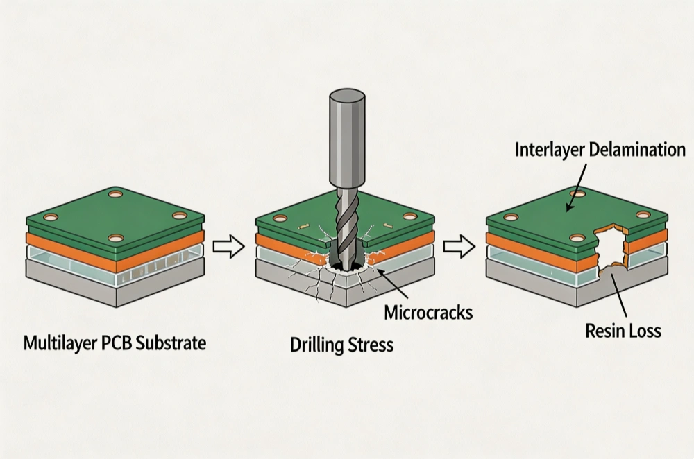
Drilling can create heat, smear, burrs, tool impact, and microcracks. Poorly controlled hole preparation or desmear can leave a damaged interface that later opens during plating, soldering, or thermal cycling. Routing, depanelization, screw fastening, connector insertion, and bending can add mechanical stress at board edges, slots, cutouts, and large plated holes.
Mechanical damage often interacts with thermal stress. A board may survive the first assembly pass but fail after repeated reflow because a drilling-induced microcrack has become a stress concentrator. Inspect edge quality, hole walls, routing features, and support conditions rather than assuming a later thermal failure began in the oven.
5. Material mismatch or inadequate design margin
A material is only suitable in the context of the application and construction. Risk can increase when the selected resin system, glass style, copper weight, layer count, board thickness, or thermal environment does not match the process and reliability requirement.
Design-related contributors include:
- abrupt changes in copper density or large unbalanced copper areas;
- tight slots, cutouts, or edge features that concentrate stress;
- thick/heavy components that bend the board during assembly or service;
- a stack-up that places a weak interface at a high-strain location;
- insufficient keep-outs around plated holes, depanelization routes, or fasteners;
- a board specified for repeated thermal cycling without validating z-axis behavior.
Core and prepreg selection are part of the stack-up rather than interchangeable layers. For high-temperature designs, a high-Tg PCB option may be relevant, but material choice still has to be verified against the complete process and operating profile.
6. Reflow, soldering, and rework
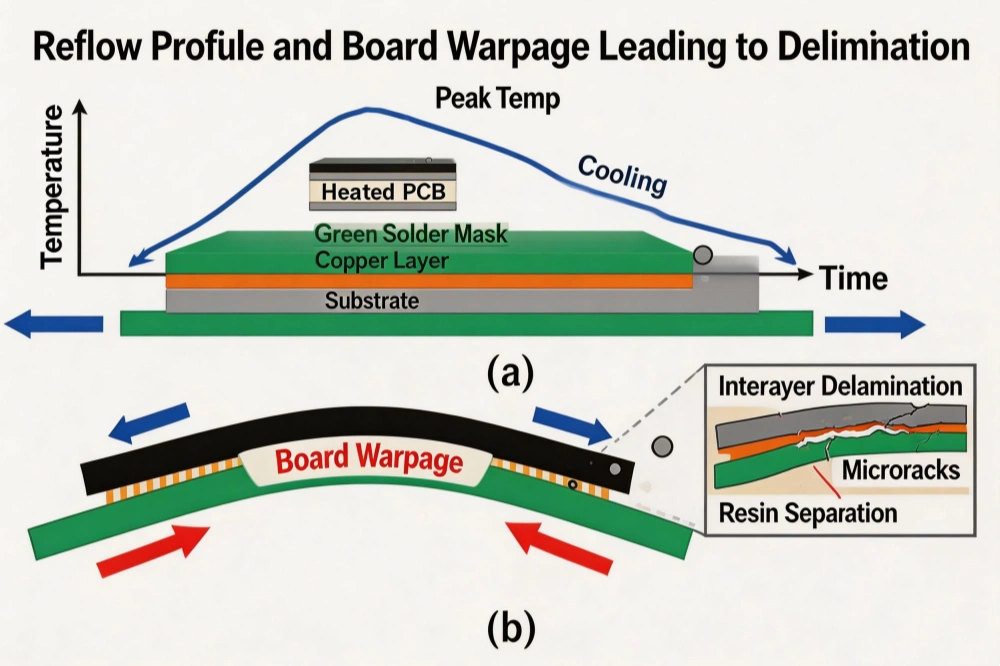
PCB delamination during reflow is usually a combined moisture-and-thermal-stress event. A board enters the oven with absorbed moisture or a pre-existing weak interface; the profile then drives rapid expansion and softening through the laminate. If the profile has an excessive ramp, peak, or dwell for that material, or if the board is exposed to more thermal passes than qualified, the separation can open.
Do not copy a profile from another product. Profile the actual board at representative locations, including thick copper regions, large thermal masses, and areas near sensitive interfaces. Confirm the material’s process window, the number of planned thermal passes, and the handling condition of the boards before soldering. GreatPCB’s reflow soldering process guide is a useful companion for reviewing the process sequence.
Rework can be more damaging than the first pass because local heating is less uniform and the board may already have accumulated moisture or mechanical damage. Define rework limits, localized preheat requirements, and inspection criteria before production.
Need help with laminate selection, DFM, or delamination analysis? GreatPCB supports global PCB manufacturing and process control.
What are the signs of PCB delamination?
Visible signs of PCB delamination can include a blister, raised laminate, edge lifting, a pale or discolored region, surface bubbling, or a separation around a hole or cutout. These signs are useful, but they do not define the full extent. Internal delamination can exist without a visible mark, and a white spot can be measling rather than a broad layer separation.
Use a staged diagnosis:
- Visual inspection: Examine both sides, edges, holes, slots, and the area around large thermal features under suitable magnification. Photograph the location and board revision.
- Electrical screening: Check continuity, insulation resistance, impedance-sensitive nets, and functional behavior where appropriate. A passing electrical test does not clear an internal laminate defect.
- Microsection or cross-section: Cut a representative coupon or failed board through the suspect region. Look for a gap, resin crack, poor wet-out, copper-interface separation, void, or plated-hole damage.
- Acoustic or non-destructive inspection: Scanning acoustic microscopy can help locate internal interfaces or voids without immediately destroying the board, when the laboratory and construction are suitable.
- Thermal or environmental reproduction: Reproduce the suspected stress with a controlled process or qualification test only after the failure mode and acceptance criteria are defined.
Record the layer location, board area, distance from the edge, relation to copper pattern, thermal exposure history, and whether the defect is isolated or lot-wide. That information separates a material/lamination problem from a local handling or assembly problem.
Does PCB delamination affect reliability?
Yes. The effect depends on the location, size, continuity, and growth potential of the separation, but a delaminated board should be treated as a reliability concern until it is characterized. Possible consequences include:
- changes in dielectric thickness or local dielectric constant, affecting impedance and high-speed signal behavior;
- reduced mechanical strength and resistance to vibration, flexing, or connector loading;
- copper-interface separation, opens, intermittent connections, or reduced solder-joint support;
- increased thermal resistance or a disrupted heat path;
- moisture and contamination pathways that can accelerate insulation degradation;
- higher stress at plated through holes and the possibility of later barrel or interconnect failure.
The correct disposition is product-specific. A cosmetic, isolated condition on a noncritical prototype is not judged the same way as a layer separation near a high-current path, controlled-impedance pair, BGA escape, plated hole, or safety-related circuit. In other words, PCB reliability depends on where the defect is, how large it is, and whether its environment can make it grow.
How can PCB delamination be prevented?
Prevention works best when it begins before fabrication and continues through assembly.
Select and qualify the material
- Specify the resin system and construction, not only “FR-4.”
- Review Tg, Td, z-axis CTE, moisture absorption, copper adhesion, dielectric thickness, and the supplier’s processing guidance.
- Confirm compatibility with the solder alloy, number of reflow/rework passes, operating temperature, and environmental cycling.
- Keep material lots and approved stack-ups under change control.
Control stack-up and design stress
- Balance copper and avoid abrupt stiffness or density changes where practical.
- Review cutouts, slots, edge routing, fasteners, and large holes as mechanical stress features.
- Give the fabricator the actual thermal and reliability requirements during DFM, not after the first failure.
- Validate high-Tg or low-CTE materials with the full stack-up; a material label alone is not a qualification.
Control lamination and fabrication
- Use the approved prepreg/core combination and verify resin fill.
- Control surface preparation, cleanliness, vacuum, pressure, temperature, cure, and registration.
- Monitor drilling parameters, tool life, desmear, plating, routing, and depanelization.
- Use coupons, microsections, and the applicable IPC qualification or acceptance tests to verify the process.
Control moisture and storage
- Store laminate and finished boards in the conditions specified by the material supplier.
- Seal or protect opened materials; track exposure time when the risk warrants it.
- Use an approved conditioning or bake process when required, and document the decision.
- Do not bake blindly: excessive heat or repeated baking can affect finishes, solderability, and material condition.
Control reflow and assembly
- Profile the actual board, not just the oven recipe.
- Keep ramp, peak, dwell, and thermal-pass count inside the approved material/process window.
- Support large or flexible panels to limit bow and twist.
- Control rework heating and inspect boards after unusual thermal exposure.
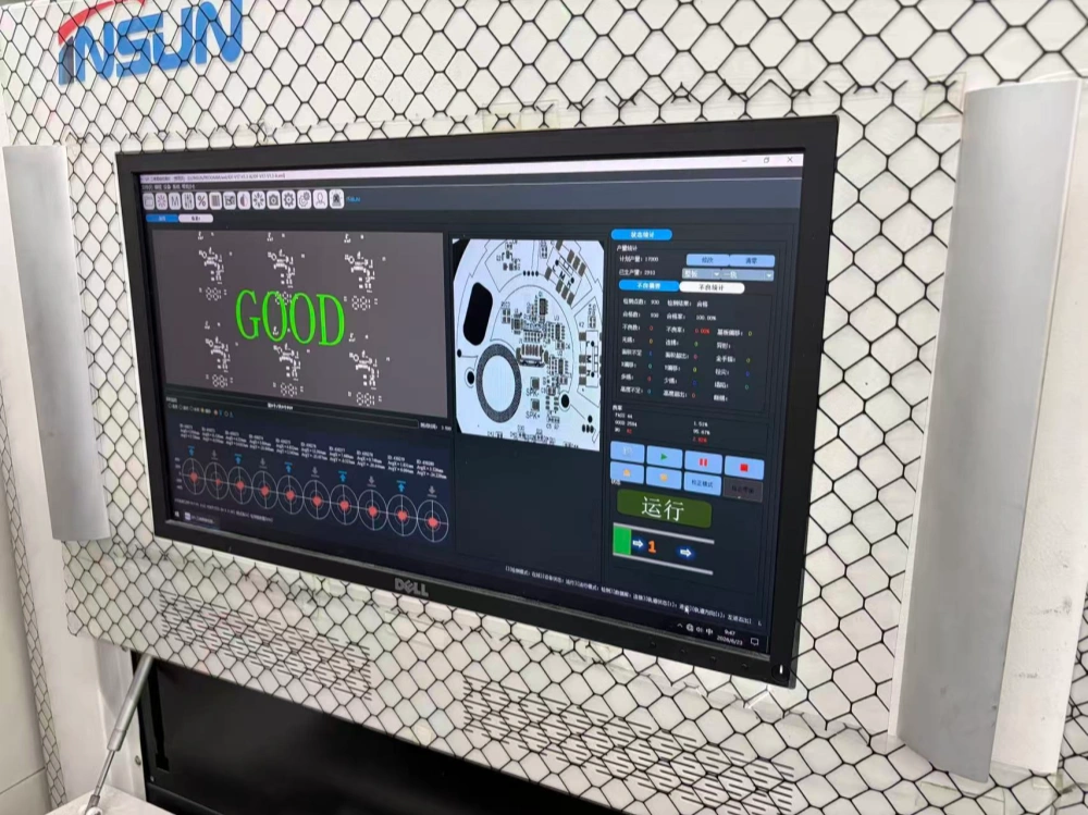
- Use solder-paste inspection (SPI), automated optical inspection (AOI), X-ray where the construction and defect call for it, and appropriate electrical or functional tests to screen assembly quality. These methods can identify solder or component defects and some void conditions; they do not, by themselves, prove that internal laminate interfaces are bonded.
GreatPCB’s PCB testing page describes visual, electrical, environmental, mechanical, X-ray, impedance, and EMC test categories. Select only the methods that can detect the failure modes relevant to your construction; “100% inspection” is not a substitute for a defined control plan.
Can PCB delamination be repaired?
Sometimes a board can be cosmetically stabilized or locally reworked, but a multilayer PCB with confirmed internal delamination is usually not considered fully repaired by injecting adhesive or pressing the area flat. The original bond, resin distribution, dielectric geometry, and reliability history cannot be assumed to have been restored. Adhesive repair can also conceal the defect and make later analysis harder.
Use this disposition logic:
- Stop and quarantine the affected lot or board family.
- Confirm the defect with cross-section, acoustic inspection, or another suitable method.
- Identify the root cause: moisture condition, laminate lot, lamination record, drilling, handling, reflow, or rework history.
- Ask the fabricator and end-product owner to approve disposition. Scrap and replacement are often the correct choices for production or safety-critical hardware.
- Allow a controlled repair only when the application, defect location, repair process, and subsequent verification are explicitly qualified. A repaired prototype is not evidence that the production process is acceptable.
What should a manufacturer provide when investigating delamination?
For a meaningful root-cause analysis, request more than photographs. The package should include:
- board drawing, stack-up, material and lot information;
- prepreg/core construction and lamination recipe or traceability;
- moisture storage and conditioning records;
- drilling, desmear, plating, routing, and depanelization records where relevant;
- reflow and rework profiles, thermal-pass count, and board support details;
- cross-sections or non-destructive inspection images through the defect;
- defect Pareto by lot, panel, layer, and location;
- containment, corrective action, and verification evidence.
This is where a manufacturer’s quality system becomes visible. A credible investigation explains how the evidence supports the proposed root cause and how the corrective action will prevent recurrence. It does not simply attribute every failure to “high temperature” or “bad material.”
Working with a manufacturer that provides documented lamination, drilling, and reflow records is essential for reliable PCBs.
FAQ: PCB delamination questions engineers ask
Reflow can expose moisture or a weak laminate interface to rapid heating, high temperature, and repeated expansion/contraction. Absorbed moisture can generate internal vapor pressure, while resin softening and z-axis expansion increase strain. If the board construction or bond lacks enough margin, the interface opens. The correct diagnosis requires the material data, storage history, board profile, and cross-section evidence.
Not necessarily. A low or poorly matched Tg can reduce thermal margin, but delamination can also result from moisture, weak lamination, contamination, poor drilling, copper imbalance, excessive thermal passes, or mechanical damage. Tg is one input; review Tg, Td, z-axis CTE, resin system, construction, and process controls together.
Delamination is a separation of bonded layers or interfaces. Measling is typically a small light spot or cross-shaped resin/glass crack or separation around glass bundles. Measling may be limited and judged under a product-specific acceptance class, while continuous delamination, blistering, or separation near critical features is a more direct reliability concern. Confirm the condition by inspection or microsection rather than by appearance alone.
It may pass a functional test temporarily, especially when the separation is internal or does not yet cross an electrical path. That does not prove reliability. Delamination can grow during later reflow, thermal cycling, vibration, or humidity exposure. Characterize the location and extent, then use the product owner’s acceptance and qualification requirements to decide whether to rework, requalify, or scrap the board.
Start with visual inspection of surfaces, edges, holes, and cutouts. Use electrical checks to identify opens or insulation changes, but do not treat a pass as proof that the laminate is sound. Microsectioning reveals the actual interface and resin/glass condition; scanning acoustic microscopy can locate some internal separations non-destructively. Select the method based on board construction and failure hypothesis.
Baking or controlled conditioning can reduce moisture-related risk when performed according to the laminate and assembly supplier’s instructions. It cannot correct weak bonding, contamination, poor lamination, damaged holes, or an unsuitable reflow profile. Bake decisions should consider material type, board thickness, finish, exposure history, and the risk of affecting solderability or other properties.
There is no single universal step. The highest-value approach is to control the chain: qualify the material and stack-up, protect it from moisture, verify lamination and drilling, profile the actual board, limit thermal passes, and use inspection capable of finding the suspected defect. Root-cause evidence is more useful than choosing a higher Tg number without validating the process.
Need a reliable PCB partner? GreatPCB supports global customers with controlled lamination, DFM, testing, and failure analysis.
Table of Contents
- What is PCB delamination?
- Why does PCB delamination happen?
- What are the signs of PCB delamination?
- Does PCB delamination affect reliability?
- How can PCB delamination be prevented?
- Can PCB delamination be repaired?
- What should a manufacturer provide when investigating delamination?
- FAQ: PCB delamination questions engineers ask
Related Posts
PCBA Prototype
September 8, 2026