
PCB fabrication · Engineering review · Optional assembly
PCB PrototypeManufacturing
Turn your PCB design into boards you can evaluate, assemble, and refine—before committing to production.
GreatPCB supports bare PCB prototypes and assembled prototypes, with engineering review of your files, materials, stackup, and test requirements. Send your design package to define a practical manufacturing route and get a project-specific quotation.
Have a deadline? Include your required arrival date and delivery destination.
Build for the next decision
Prototype Workflow
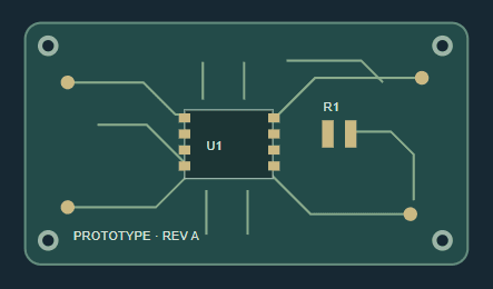
Review files Confirm specification Build & inspect
Illustrative PCB layout. Your board is manufactured to its approved project specification.
Engineering file review
Resolve manufacturing questions early
Bare board or PCBA
Choose the scope your prototype needs
Material & stackup coordination
Align fabrication with design intent
Prototype to production
Retain an approved manufacturing baseline
Choose your build
PCB Prototype Services
A PCB prototype is a small initial build used to evaluate a board design before repeat manufacturing. The right order depends on what you need to learn: mechanical fit, assembly feasibility, circuit operation, or performance under operating conditions.
01 / BARE PCB
PCB Fabrication
Order the unpopulated circuit boards for in-house assembly or a separate assembly partner. Define the board construction, finish, holes, outline, and electrical test requirements in the fabrication package.
Best fit: layout iterations, enclosure checks, and teams that already manage component assembly.
02 / ASSEMBLED PCB
PCB Assembly
Combine fabrication with component sourcing, SMT/THT assembly, and agreed inspection or testing. Add a BOM, placement data, assembly drawings, and firmware or test instructions where needed.
Best fit: powered circuit evaluation and designs with packages that are difficult to assemble by hand.
03 / REPEAT BUILD
Low-Volume Production
Move an approved design into a small production run. Preserve the released fabrication files, material specification, assembly instructions, and acceptance criteria across repeat orders.
Best fit: pilot builds, field evaluation, and the first production batch after design changes close.
Define the deliverable first. A bare PCB order supplies circuit boards without components. Power-up, firmware verification, and product-level functional tests belong to the assembled prototype and its agreed test plan.
Board construction
PCB Types
GreatPCB offers rigid, multilayer, HDI, flex, rigid-flex, high-frequency, and heavy-copper PCB services. The manufacturing route is reviewed against your actual design; layer count, dimensions, copper weight, and feature limits are confirmed together.
Flex & Rigid-Flex PCBs
For constrained packaging and connections between rigid sections. Identify bend regions, stiffeners, coverlay, and whether the circuit bends only during installation or repeatedly in service.
Heavy Copper PCBs
For power distribution designs that require thicker copper. Review current paths, thermal conditions, spacing, and copper thickness together; copper weight alone does not establish a safe current rating.
Metal-Core PCBs
For applications such as LED modules where heat transfer is a key design consideration. Define the base material, dielectric system, mounting arrangement, and electrical insulation requirements.
Material families describe available service categories. Material grade, procurement, construction, and process feasibility are confirmed for each quotation.
Specify what matters
PCB Specifications
A layer count and board size are enough to begin a conversation, but they do not fully define a prototype. The following details determine how the board will be made and whether it represents the design you intend to validate.
| Specification | What to provide | Why it matters |
|---|---|---|
| Layers & stackup | Layer order, copper weights, dielectric construction, finished thickness | Defines the physical board and its signal reference environment. |
| Material | Laminate grade or electrical/thermal requirements; substitution policy | A material change may affect impedance, loss, thermal behavior, and validation results. |
| Holes & vias | Finished hole sizes, PTH/NPTH distinction, drill spans, fill/cap requirements | Clarifies plating, component fit, and the via manufacturing sequence. |
| Controlled impedance | Target, tolerance, layer, net or geometry reference, test/report request | Connects your routing to a manufacturable stackup and verification method. |
| Surface finish | Finish type and any contact, storage, or soldering constraints | Influences pad planarity, solderability, handling, and assembly scheduling. |
| Outline & panel | Dimensioned outline, slots, cutouts, critical tolerances, panel requirements | Supports enclosure fit, depaneling, and the assembly process. |
| Acceptance & records | Applicable acceptance criteria, test coverage, and required documents | Makes inspection expectations part of the order rather than a later assumption. |
Use a manufacturing drawing to call out critical features. If a requirement appears in more than one file, keep the revision and value consistent across the entire package.
Manufacturing review
DFM Review
DFM—design for manufacturing—checks whether your released design can be produced with the selected process. A useful review translates a warning into a specific decision: adjust a feature, change the construction, or clarify a manufacturing instruction.
GreatPCB reviews the submitted design package for manufacturability. Unresolved questions should be closed against the approved revision before fabrication begins.
If assembly is included, the review also considers component data, footprints, placement access, and panel handling. This assembly review is often described as DFA, or design for assembly.
DFM Checklist
DFM complements design verification. It addresses manufacturing risks. Circuit correctness, signal integrity, firmware behavior, and compliance testing still need an appropriate engineering validation plan.
Electrical performance
Stackup & Impedance
Controlled impedance depends on more than trace width. Dielectric thickness, material properties, copper geometry, and the reference plane all contribute. Changing the layer construction after routing can change the electrical behavior you are trying to evaluate.
For high-speed or RF designs, include the impedance targets and identify the relevant layers or nets. Agree a manufacturable stackup, then confirm any proposed geometry adjustment before releasing the board.
Also check the signal return paths. A correct impedance target does not compensate for a discontinuous reference plane. Prototype validation should use a construction representative of the intended production design.
Four-Layer Stackup Example
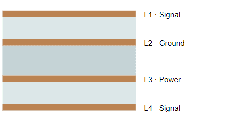
Conceptual example, not a recommended stackup for every circuit. Layer functions, dielectric thicknesses, and materials must be selected for your design.
Assembly readiness
Surface Finishes
Choose the finish around component pitch, soldering process, storage, and contact requirements. The lowest board price can be a poor trade if the finish complicates the assembly or test process.
| Finish | Useful characteristics | Selection considerations |
|---|---|---|
| Lead-free HASL | A mature solder finish often considered for general-purpose layouts. | Pad planarity is less uniform than ENIG or OSP; review suitability for fine-pitch devices and thin boards. |
| ENIG | A flat nickel/gold finish suited to many fine-pitch assembly applications. | Costs more than basic finishes. It is different from wear-resistant hard gold used on mating contacts. |
| OSP | A thin organic coating that protects copper while preserving a flat pad surface. | Handling, storage, soldering sequence, and probe contact need attention. It is unsuitable for wear-resistant edge contacts. |
| Other specified finishes | Immersion silver, immersion tin, hard gold, or ENEPIG may address particular needs. | Confirm process availability and specify where the finish is required. An edge connector may need a different finish from the solder pads. |
For RF designs, review the finish as part of the electrical construction. For repeated connector insertion, specify the contact plating requirement separately. Available finishes and processing details are confirmed during quotation.
How the service works
Manufacturing Process
01
Send Files
Provide fabrication files, board requirements, quantity, and schedule. Include assembly data if you need populated boards.
02
Engineering Review
Confirm the stackup, materials, finish, test scope, and manufacturing changes. Approve the final data revision and quotation.
03
PCB Manufacturing
Fabrication follows the approved construction. Multilayer boards involve imaging, etching, lamination, drilling, plating, mask, finish, and profiling; the sequence varies with the technology.
04
Testing & Delivery
Complete the agreed inspection and electrical testing, then pack and ship. For PCBA, add component assembly and the specified assembly test activities.
Know what is verified
Quality Control
Different checks answer different questions. Specify the test method, coverage, acceptance limits, and records you need when requesting a quotation.
Optical & Dimensional Inspection
Optical inspection checks circuit features against design data. Dimensional and visual checks address the outline, hole position, finish, solder mask, and other drawing requirements. These checks do not establish powered circuit performance.
Bare-Board Electrical Testing
Continuity and isolation checks detect open or shorted connections. Flying probe testing is often useful for prototypes because it avoids a dedicated test fixture; the chosen method depends on the board and order scope.
Impedance Testing
When required, agree coupon construction, measurement method, tolerance, and report delivery. A coupon measurement assesses representative transmission-line geometry; it does not validate every aspect of the assembled system.
Assembly & Functional Testing
For populated prototypes, inspection may include SPI, AOI, or X-ray as appropriate to the package risks. Functional testing needs defined power conditions, firmware, interfaces, expected results, and any fixtures or loads.
Request the records your evaluation needs. Identify electrical test reports, impedance results, dimensional checks, or material documentation in the RFQ. Additional reliability or environmental tests require a separately agreed scope.
Cost & lead time
Cost & Lead Time
Cost Factors
Board area, quantity, layer construction, material, copper weight, feature density, finish, and special processing all affect the fabrication route. Tooling, inspection, and requested reports may also influence the total.
For assembled prototypes, component pricing, sourcing, placement work, programming, and test preparation add separate costs. Compare quotations using the same specification and delivery scope.
Lead Time Factors
File clarification, material procurement, sequential lamination, via processing, inspection, and logistics can each add time. Assembly also depends on component availability and the readiness of firmware and test instructions.
Specify a required arrival date, not just “urgent.” Distinguish engineering review, manufacturing completion, shipment, and delivery when agreeing the schedule.
Reduce cost without weakening the experiment. Use standard materials and practical design rules where they meet the circuit requirements. Keep the construction representative when validating electrical or thermal performance; a cheaper, materially different prototype can answer the wrong question.
Quotation checklist
Required Files
PCB Fabrication Files
An IPC-D-356 netlist can support an independent connectivity comparison when available. Confirm alternative data formats with engineering before submission.
PCB Assembly Files
Keep one released revision. Export the fabrication, BOM, placement, and drawings from the same approved design. Mark superseded files clearly.
Keep the learning
Prototype to Production
A working prototype is a development milestone. Before repeat manufacturing, close the changes that affect fabrication, assembly, and acceptance so the next batch reproduces the approved design.
RELEASE
Design Release
Record the fabrication files, drawing, material specification, stackup, BOM, and firmware version that produced the accepted prototype.
CHANGE CONTROL
Revision Control
Document layout changes, material substitutions, and process changes. Reassess affected features rather than assuming earlier test results still apply.
REPEATABILITY
Production Testing
Define the checks and pass/fail limits required for repeat orders. Adjust panelization, tooling, and test strategy as volume grows.
Your manufacturing partner
Why Choose GreatPCB?
Founded in 2002, GreatPCB has over 20 years of PCB manufacturing experience. Our service scope connects PCB fabrication with component sourcing, SMT/THT assembly, programming, and testing for customers developing and producing electronic products.
You can request bare boards for your own assembly workflow or coordinate fabrication and assembly within one project. Engineering review helps define the manufacturing specification before the build moves forward.
Coordinated Manufacturing
Tell us what you need to validate and what you will handle in-house. We can review the requested fabrication, sourcing, assembly, and testing scope together, so your quotation describes the deliverable your team expects.
Before you order
PCB Prototype FAQs
Ready for the next build?
Request a Prototype Quote
Send your released design files and tell us what the prototype needs to demonstrate. Include the board quantity, key specifications, and deadline so GreatPCB can review the manufacturing scope and prepare a quotation.
sales@greatpcb.com · Attach your files to the email before sending.
RFQ Checklist
For PCBA, also attach the BOM, placement data, and assembly instructions.