HDI PCB Design Guide
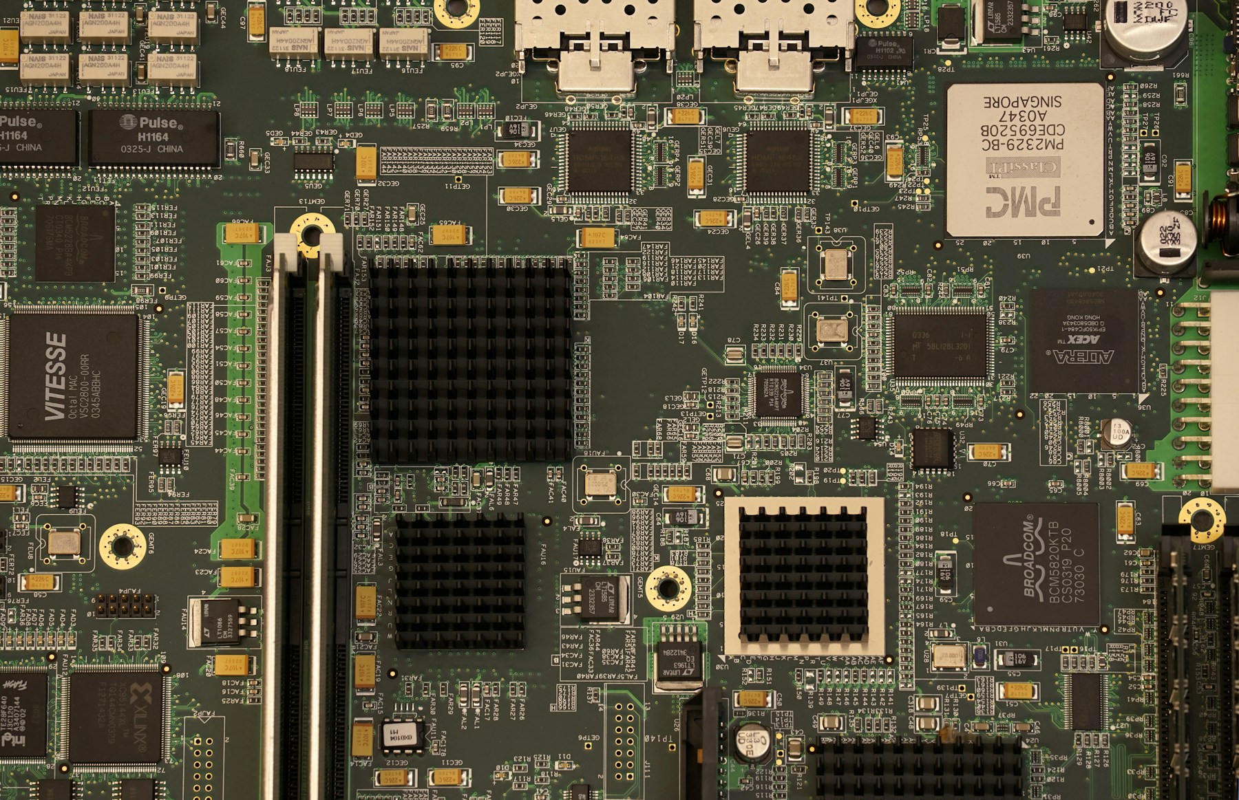
High-density interconnect (HDI) PCB design uses compact interconnects and fine routing features to make connections that a conventional layout may struggle to fit. The design task is to make those connections work together with the stackup, fabrication process and assembly—not simply to shrink every trace and via.
Start with the package pin map and the paths each signal must take. Then choose build-up layers and via structures that the fabricator can produce and that the product can validate. This guide follows that sequence, from deciding whether HDI is needed to preparing a design-for-manufacturing (DFM) review.
The dimensions used in the examples below are illustrative assumptions, not GreatPCB manufacturing limits or approved package footprints.
When Do You Need HDI?
HDI is worth evaluating when a conventional multilayer layout cannot connect the actual component pins within the board’s area and thickness limits while preserving signal and return paths. A fine-pitch BGA may add pressure, but pin assignment, escape direction, routing layers, nearby components, and board outline determine the available channels.
Before selecting a stackup, route the critical packages using their real land patterns and net assignments. Compare a conventional via-and-layer approach with a candidate HDI connection map. If the first leaves blocked inner rows, forces an unacceptable board size, or breaks electrical constraints, ask the fabricator to review viable layer transitions and process assumptions. Keep any tighter trace rules local to the package area where the map shows they are needed.
| Constraint | First validation |
|---|---|
| Dense BGA rows cannot escape on available layers | Route the real pin map; count open channels and identify blocked pins. |
| Board outline or thickness is fixed | Compare routed area and layer reach against both constraints. |
| High-speed nets compete with pin escape | Check interface routing, reference continuity, and return paths together. |
| Power pins crowd signal routes | Verify the power-delivery network before accepting a layer-reduction tradeoff. |
Use HDI when this comparison shows a specific connectivity or form-factor gain that can be reviewed with the fabricator.

Package placement and nearby components determine how much routing space is available.
Plan the Stackup First
Read 1+N+1 and 2+N+2
Stackup planning starts with required connections and their layer spans. The notation describes build-up around a central core: 1+N+1 places N core layers between one build-up layer on each side; 2+N+2 places N core layers between two build-up layers per side.
Use the comparison to check whether available build-up levels support the intended escape paths before setting detailed dimensions.
For six layers, 1+4+1 has a four-layer core (L2–L5) and one build-up layer per outer side (L1, L6); 2+2+2 has a two-layer core (L3, L4) and two build-up layers per side. Both total six copper layers but arrange core and build-up differently. The notation does not give the exact lamination-cycle count, each hole’s span, or an IPC Type. Define spans from actual connections and confirm the process sequence with the fabricator. See GreatPCB’s PCB stack-up overview when preparing that discussion.
For example, Type I and Type II can each have one build-up level per side; the presence of buried vias distinguishes those constructions. The numeral in an IPC Type label therefore does not directly state the build-up count.
These are structural examples, not approved fabrication designs. Material, dielectric thickness, registration, drilling, filling, and repeated build-up operations affect what is practical.
Map the Layer Connections
Map the layers before assigning vias. In 1+4+1, outer blind microvias may connect L1–L2 and, mirrored, L6–L5. Reaching farther requires another defined transition or a longer via span. In 2+2+2, top-side transitions may be L1–L2 and L2–L3, mirrored at L6–L5 and L5–L4. Through vias may span the stack; buried vias join selected internal layers.
Write each path in order—for example, L1 to L3 through two adjacent-layer transitions—and check that every transition lands on an available layer. The map shows whether the route uses one hole or several, where layers change, and which operations the board shop must sequence. Align it with the schematic and routing plan; “order” alone does not define hole depth.
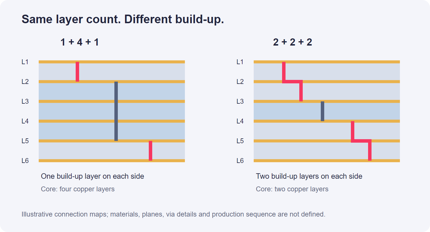
Illustrative six-layer build-up connection maps; not approved fabrication stackups. View full-size diagram.
Choose the Microvia Structure
Staggered, Stacked and Skip Microvias
Map the layer connections first. Adjacent-layer microvias join neighboring layers. Staggered vias step sideways between build-up layers; stacked vias align vertically, saving routing area while adding registration and plating interfaces to control. A skip microvia crosses an intermediate layer to a deeper target, reducing transitions when its span and land suit the process. Blind vias can span more than one layer; labels alone do not qualify a stackup.
| Structure | Layout effect | Check with fabricator |
|---|---|---|
| Staggered | More lateral room | Offset lands and registration |
| Stacked | Compact escape | Alignment, plating sequence, evidence |
| Skip | Deeper reach, fewer transitions | Span, dielectric, target land |
Choose the simplest structure that reaches required layers from the actual pins. Check the full stackup: each transition needs a valid land, and tight geometry reduces registration margin. Have the fabricator review spans and stacked interfaces before routing is fixed.
Via-in-Pad and Filling
Via-in-pad places a via inside a component land; it does not prescribe filler. An open land hole can disrupt soldering, so specify the finished surface for assembly.
Copper-filled laser microvias use electrodeposited copper; the specified finish may include planarization and a copper cap. A mechanical hole can be resin-filled, cured and planarized, then capped for a flat solderable surface. Its plated barrel remains the electrical path. These are distinct process choices, not a quality ranking.
On the drawing, state hole type and span, electrical connection, fill, and cap or flatness intent. Ask about process sequence, registration and surface control, plus inspection or qualification evidence for this design. For stacked structures, confirm how the shop forms and inspects each interface. Confirm land and finish with assembly; “via-in-pad” alone is incomplete.
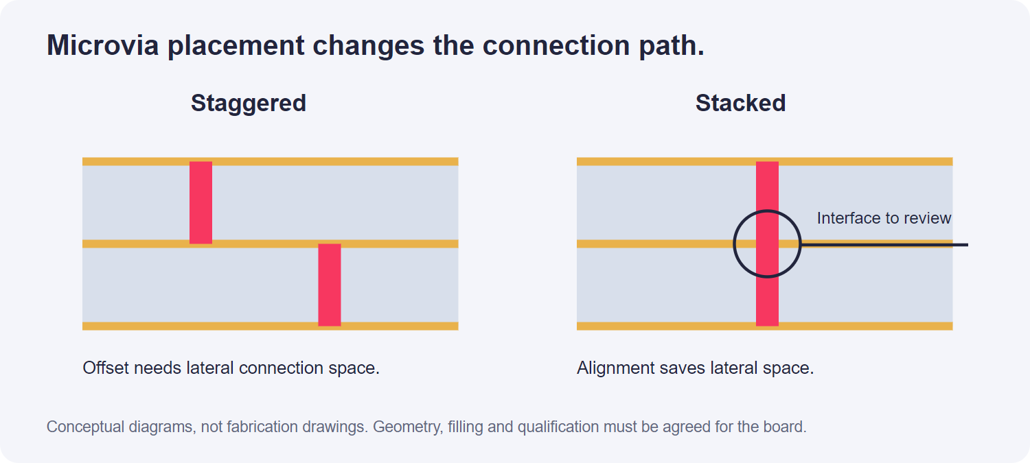
Conceptual staggered and stacked microvias; filling, landing geometry and qualification must be specified separately. View full-size diagram.
Work Out the BGA Escape
Start with the Pin Map
Build the escape from the package’s land pattern and pin map. Mark signal pins by interface and routing constraints, separate power and ground connections, and exclude no-connect pins from the route count. Then identify which outer rows can leave the package directly and which inner rows need channels between lands or a transition to another layer. A sample fanout for one device only works when its pin assignment and electrical requirements match; pitch alone cannot tell you how many routes will fit.
Check the Routing Channel
Hypothetical geometry (illustrative only): At 0.50 mm pitch with a 0.25 mm copper land diameter, adjacent lands leave a 0.25 mm gap. A 0.075 mm trace with 0.075 mm clearance on each side occupies 0.225 mm, leaving a nominal 0.025 mm margin in that gap. This is a geometry check, not manufacturing qualification. It excludes via lands, registration and etch tolerances, solder-mask effects, and assembly constraints; actual rules must be agreed for the selected stackup and process.
Choose the Escape Route
For outer rows, a dog-bone route can move a signal from its land to an offset microvia, then continue on another layer. It uses lateral room, so check neighboring vias and remaining channels against the full pin map. For blocked inner rows, via-in-pad can place the layer transition at the land and preserve surface routing space. That choice requires a defined fill, cap, and surface-flatness plan that works for both fabrication and assembly; it is not automatically needed for every BGA pin.
Use local fine-line rules only where the routed map needs them. Apply trace width and clearance by layer and package region, and verify the route after adding via lands and all adjacent-net constraints. If the escape works only after dropping a required electrical constraint, revise the stackup or escape structure before routing the rest of the board. Record the pin groups, layer transitions and unresolved channels for fabricator review.
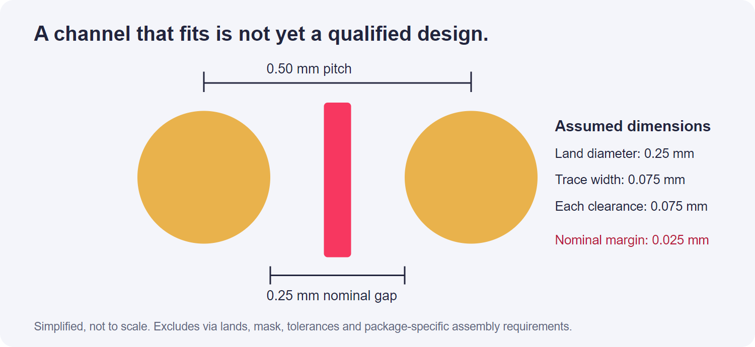
Illustrative BGA channel arithmetic; not to scale and not a fabrication approval. View full-size diagram.
Set Manufacturing-Aware Design Rules
Trace and Clearance Rules
Treat each HDI rule as a process-specific design input, not a board-wide slogan. Define trace width and clearance by layer, copper condition, and routing region: a dense BGA escape may need a local rule that should not be imposed on every signal layer. Check the complete combination with the fabricator, since etching, copper distribution, build-up sequence, and registration interact. A CAD rule passing only confirms nominal geometry; it does not establish manufacturing margin.
Microvia Geometry
For a microvia, distinguish the capture land at the drilled side from the target land that receives the connection. State the intended layer span and both land dimensions, then ask the fabricator to confirm the registration allowance and how it evaluates a reliable landing. Dielectric thickness and via geometry must be reviewed together. As a hypothetical arithmetic example, 60 µm depth divided by a 100 µm bore gives an aspect ratio of 0.6. This is not a recommended limit. The fabricator must approve the measurement basis, especially whether depth and bore refer to nominal dimensions, finished dimensions, or a particular point in a tapered bore, and confirm the applicable process window.
Confirm the Design Rules
| Rule to define | Inputs to provide | Confirm and record |
|---|---|---|
| Trace and clearance | Layer, copper condition, routing region, net class | Fabricator: combined feature and process margin; controlled constraint set |
| Microvia landing | Layer span, dielectric depth, bore profile, capture and target lands | Fabricator: registration and measurement basis; approved stackup and drill table |
| Solder mask | Side, land opening, mask web or clearance intent, via-in-pad treatment | Fabricator and assembly team: registration and surface plan; fabrication notes |
Send the same controlled stackup, drill table, copper assumptions, and mask data with the design package. Record replies against the relevant layer and feature; a generic “DFM approved” does not resolve an unspecified measurement basis or land geometry.
Protect Signal, Power and Assembly Paths
Signal and Power Paths
An escape route is not complete when every BGA pin has a destination. Check each high-speed route’s reference plane and return-current path at layer changes. When its reference changes, plan a nearby return transition with the signal via. Review controlled-impedance geometry against interface needs and package guidance; a fanout from a different device may not apply.
Antipads also affect plane connectivity. Closely spaced openings may narrow copper necks or divide a plane region, changing power paths as well as return paths. After adding transitions, inspect plane continuity and the power-delivery network. Size antipads and any plane clearances for the local electrical need; avoid global changes. Let the pin map and layer use guide this review.
Land Patterns and Via-in-Pad
For the land pattern, distinguish SMD (solder-mask-defined) from NSMD (non-solder-mask-defined). Here, SMD describes how the solder mask bounds exposed copper, not surface-mount technology. Follow the package vendor’s recommendation and check mask registration against the selected process. For via-in-pad, specify hole type, electrical connection, fill or cap, and flatness together. An open hole can draw solder from a joint; an approved filled, planar surface changes the assembly interface.
Inspection and Thermal Planning
Plan inspection and rework for hidden BGA joints. Fine-pitch assembly depends on land pattern, mask alignment, stencil process, and repair access, so confirm the inspection approach with the assembler. See GreatPCB’s BGA assembly guidance for assembly considerations. Treat heat flow as a separate design path: microvias can conduct heat, but arbitrary vias do not replace connections to useful copper or a package-level thermal plan.

Electrical paths, package clearances and assembly access must be reviewed together.
Design for Microvia Reliability
Microvia Interface Failures
Reliability review starts at the copper interface where a microvia lands on its target pad. If that interface is weak, heating can separate it and interrupt continuity. In some reported cases, cooling lets the surfaces touch again, so a room-temperature continuity check after assembly may pass even though the connection opened during a hot cycle. Electrical screening is useful for opens present at the time of test; by itself, it does not show how a structure behaves under the product’s thermal stress.
Qualify the Via Structure
IPC’s 2019 industry warning documented microvia failures that emerged after bare-board acceptance. It is a historical warning, not a current mandatory standard clause or evidence that stacked microvias inevitably fail. Stack choices should follow a qualified process. Stacked structures can save routing area, while staggered structures need lateral room; either can be reliable when materials, fill, plating and the target-pad interface are controlled and validated for the intended use. The question is whether the fabricator can repeatedly build and inspect the exact sequence and interface.
Plan Reliability Validation
During DFM review, put these items on the agenda:
- Share the stackup, via sequence, fill and cap requirements, and ask how registration, plating uniformity and filled-via planarity are controlled across the build.
- Describe the product’s thermal duty, including assembly reflow, expected operating cycles and any rework exposure. Check that the materials and construction are suitable for that history.
- Agree with the fabricator on representative coupons and a test plan before release. Define what structure the coupons represent, what stress they will see, whether continuity is monitored during stress or only afterward, and what evidence constitutes acceptance.
- Record the agreed test conditions and acceptance criteria with the fabrication package, then confirm that production lots can be traced to the approved construction.
A coupon result applies to the structure and conditions tested. Use it with process evidence and the product’s duty profile; do not treat a passing room-temperature check as proof of long-term reliability.
Review Cost and Complexity
Process Steps and Margin
An HDI quote should reflect the complete fabrication route, not nominal layer count. After the core is made, each build-up stage may require dielectric lamination, laser drilling, imaging and plating, with registration checks. For a flat via-in-pad land, specify copper or resin fill and any planarization or copper cap; these require distinct process steps.
These operations interact. Tighter lands and fine line/space leave less room for registration and etch variation; adding repeated stages can make control more demanding. Fill planarity, plating uniformity and thin-panel handling also matter across the sequence. Extra stages or rework may affect yield and cycle time, so neither should be inferred from layer count alone—or reduced to a blanket HDI price multiplier.
Compare Fabrication Routes
Start with the least complex HDI structure that meets package escape and power-distribution needs. For a useful comparison, send each fabricator the same layer map, via spans and types, fill/cap/flatness intent, materials and copper requirements, local fine-feature rules, board thickness, order quantity, and prototype/production qualification plan. Ask them to compare the proposed routes and identify process assumptions before design freeze. If production changes the materials or via sequence used in the prototype, review whether the earlier qualification evidence still represents the new construction.
HDI DFM Checklist
Before release, turn assumptions into written fabrication and assembly decisions. Close each item with an owner, an answer, and a matching revision.
- Stackup: Attach the approved layer sequence; identify material grades, finished copper weights, and dielectric thicknesses by layer. Note substitutions requiring approval.
- Via connectivity: Supply a layer-to-layer table listing every drill pair, blind or buried span, and stacked or staggered transition. For each via-in-pad, state electrical connection, fill, cap, and surface condition; ask the fabricator to confirm the sequence.
- Impedance and geometry: Tie each controlled net or class to its target, tolerance, reference plane, and trace geometry. Confirm width, spacing, copper condition, and dielectric assumptions against the stackup; call out any impedance coupon in the fabrication notes.
- Rules and registration: Set trace and clearance rules by layer and routing region. Show capture and target lands, transition registration allowance, and solder-mask opening or web intent around fine-pitch pads.
- BGA and electrical review: Check the pin map against signal, power, ground, and no-connect assignments; verify escape routes, layer changes, return paths, and plane continuity. Resolve land-pattern or mask questions with the assembler.
- Reliability acceptance: Identify a coupon representing the via sequence. Agree on thermal stress conditions, continuity monitoring, acceptance criteria, and evidence to retain with lot records.
- Release data: Match fabrication notes, stackup, drill files, netlist, and outputs to one controlled revision. List open exceptions; generic DFM approval does not close them.
For a focused manufacturing review of the proposed HDI construction, contact GreatPCB about HDI PCB manufacturing.
FAQs
How is an HDI PCB different from a multilayer PCB?
HDI uses finer features and build-up connections, often laser-drilled microvias, to route dense packages. “Multilayer” only means multiple conductive layers; HDI boards are multilayer too. The label alone sets no layer count, via size, or universal rule.
Does second-order HDI mean one via crosses two layers?
No. Order describes the build-up arrangement, not one hole’s span. A microvia often joins adjacent layers; longer routes may use a sequence of vias and lands. Mark each connection’s start and end layers on the stackup.
Must microvias be stacked?
No. Stacked vias save lateral space; staggered vias need room for their offset. Choose based on escape routing, layer reach, and the fabricator’s qualified process. Confirm landing geometry and reliability for the selected structure.
Is via-in-pad filled only with resin?
No. Depending on hole type and process, fill may use plated copper or resin. Resin may need planarization and a cap for a flat surface. Specify the electrical path, fill, cap, and surface intent so assembly can assess solder-wicking risk.
Is there a universal minimum microvia or trace width?
No. Feasible dimensions depend on layer, dielectric, copper, registration, geometry, and process. Ask the fabricator to review the actual stackup and layout; generic charts are not production limits.
Can continuity testing prove long-term reliability?
No. Room-temperature continuity confirms a connection at that moment. A microvia interface may separate under heat and reconnect after cooling, escaping checks made only before and after stress. Match coupon and performance testing to the stackup, product thermal conditions, and risk.
Table of Contents
- Mikor van szükség HDI-re?
- Először a stackup megtervezése
- Válassza ki a Microvia struktúrát
- Dolgozd ki a BGA Escape-et
- Gyártástudatos tervezési szabályok meghatározása
- Jel-, táp- és összeszerelési útvonalak védelme
- Microvia megbízhatóságra tervezve
- Költségek és összetettség áttekintése
- HDI DFM ellenőrzőlista
- GYIK
Tags
Related Posts
PCBA Prototype
September 8, 2026