
Via-in-Pad PCB: When to Fill, Cap, Tent or Leave Vias Open

A via placed inside a component pad can free routing space and create a short connection to an inner layer. But that same opening may draw molten solder away from the joint during assembly. The right treatment depends on where the via is used, how it is built and what the component needs.
For a fine-pitch BGA, the priority may be a flat, solderable pad that supports a reliable ball connection. Under a QFN thermal pad, the decision also involves heat transfer, solder paste and the component manufacturer’s land-pattern guidance. In both cases, the drawing should describe the intended via treatment instead of leaving the fabricator to infer it from the hole location.
Quick answer: Via-in-pad describes where a via is located, not how it is filled. A filled-and-capped via can provide a continuous copper surface for a soldered pad; an open, tented or plugged via may be appropriate in other locations or under particular component guidance. Match the treatment to the pad, stackup and assembly requirements.
What Is a Via-in-Pad?
Via-in-pad describes a location: the via sits within a component’s land pattern instead of beside the pad. A conventional dog-bone connection uses a short trace between the pad and a nearby via. Moving that via into the pad can free space for routing around a dense footprint.
It does not describe one specific hole structure. The connection might use a plated through via, a blind via or a microvia, depending on the stackup and the layers that must connect. Nor does the name alone specify whether the hole is open, filled or covered with copper.
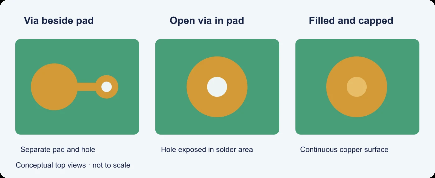
Via position and surface treatment are separate design choices. Conceptual illustration, not to scale.
Why Can an Open Via Affect a Solder Joint?
When solder paste melts, solder can flow into an open plated hole. This is called solder wicking. If too much solder leaves the pad, the component joint may have less solder than intended.
The effect is not determined by location alone. Hole size, the available solder paste, the component land pattern and the assembly process all matter. A small signal pad beneath a BGA ball also has a different soldering area and function from a large exposed thermal pad beneath a QFN.
Where an open hole creates an unacceptable risk, moving the via outside the pad or using an appropriate filled and capped structure are possible design choices. Moving the via alone does not guarantee that solder cannot reach it: the connecting trace, mask clearance and placement also matter. For thermal pads, follow the device supplier’s land-pattern and assembly guidance as well as the board manufacturer’s process requirements.
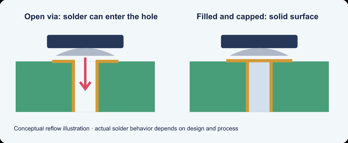
An open via can draw solder away from a pad during reflow. Conceptual illustration, not to scale.
Tented, Plugged, Filled and Capped: What Is the Difference?
These terms describe different features, and some can be combined. A filled via, for example, can also be copper capped. When ordering, specify both what happens inside the hole and what is required at the surface.
| Treatment | What happens to the via | Surface and design consideration |
|---|---|---|
| Open | The plated hole remains open. | Solder can enter an exposed hole during reflow; assess the component and process. |
| Tented | Solder mask covers a via opening. | A mask covering is not the same as a filled hole or a copper-capped solderable pad. |
| Plugged | Material blocks the opening or part of the hole. | The material, depth and coverage should be specified; plugging alone does not necessarily provide a flat copper surface. |
| Resin filled | Resin occupies the hole after the barrel is plated. | The fill and surface finish need separate definition if the via is in a solderable pad. |
| Filled and copper capped | The hole is filled and the surface is finished with a copper cap. | Creates a continuous solderable surface when properly manufactured; specify the treatment and the required sides. |
| Copper filled | Copper is deposited to fill the via structure. | Often considered for suitable microvia structures; the process depends on hole geometry and stackup. |
Manufacturers may use terms such as filled, plugged, covered and capped differently in conversation. Identify the exact vias and describe the intended structure in the fabrication drawing. IPC-4761 type designations can support communication when the applicable requirements are agreed for the order.
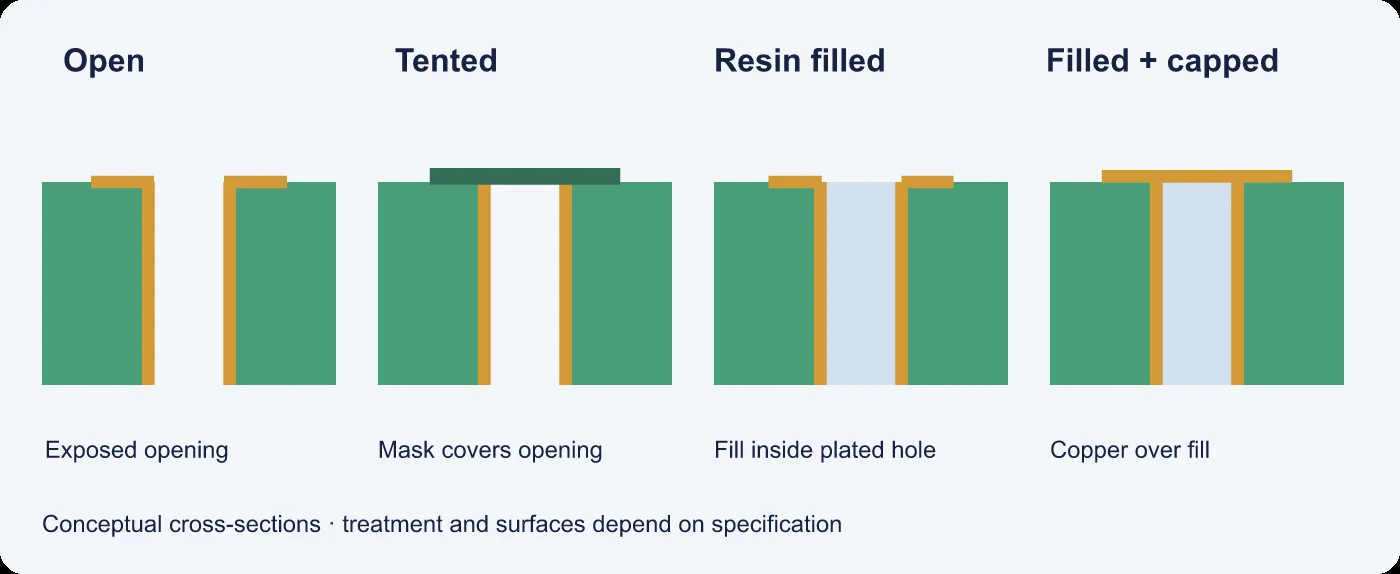
A mask covering, a filled hole and a copper cap are different features. Conceptual illustration, not to scale.
A bare circuit board showing exposed pads and holes. The image is illustrative and does not identify a specific via-in-pad construction.
BGA Signal Pads and QFN Thermal Pads Have Different Priorities
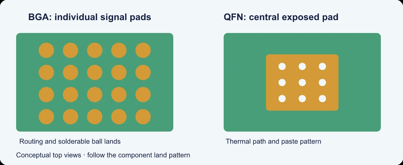
BGA signal pads and QFN thermal pads have different design priorities. Conceptual illustration, not to scale.
| Design | Why vias may be placed in the pad area | Key checks |
|---|---|---|
| Fine-pitch BGA | Free escape-routing space and connect inner balls to other layers. | Pad size, available routing, via span, solderable surface and the risk of solder wicking. |
| QFN exposed thermal pad | Connect the exposed pad to copper planes for heat transfer and, where applicable, ground. | Device land pattern, thermal-via array, solder paste coverage, solder wicking and assembly process. |
Fine-pitch BGA: routing and solderable area
As ball pitch decreases, placing a via beside each pad can consume the space needed for traces. A via in the pad may make the breakout practical, but pitch by itself does not decide the solution. Review pad size, trace width and spacing, layer count and where the signals need to go.
For a soldered BGA pad, a filled-and-capped structure can provide a more continuous surface than an open hole. The stackup also matters: a through via passes to the opposite side, while a blind via or microvia connects only a specified layer span. Our HDI PCB design guide explains how microvias and layer build-up relate to dense routing.
QFN thermal pad: heat transfer and solder paste
Thermal vias connect the exposed-pad area to copper that can carry heat away. Their number and arrangement depend on the thermal and electrical needs of the design. The solder paste pattern and the way the vias are treated also affect assembly.
As one specific example, NXP’s PwrQFN assembly guidance, AN2467, section 4.2.2.3 describes a thermal-via array with a 1.20 mm grid and a recommended via diameter of 0.30–0.33 mm with 35 µm copper plating. For its stated design, the guide also discusses tenting the top surface if the vias are not plugged by copper plating. These values belong to that PwrQFN guidance; use the actual component’s documentation and thermal analysis for your design. Confirm whether the hole size on your fabrication drawing is a drill size or a finished size instead of assuming the two are interchangeable.
Resin Fill, Conductive Fill and Copper Filling
Non-conductive resin fill occupies the space inside a plated via. The resin itself is not the electrical connection: the plated copper barrel can still connect the relevant layers. A copper cap may be added when the pad needs a continuous solderable surface.
Conductive fill uses a conductive filling material, such as a suitable copper-containing paste. Its thermal and electrical properties depend on the material and the finished structure. It should not be assumed to behave identically to a via filled by copper electroplating.
Copper filling deposits copper into the via itself. The choice depends on the via’s geometry, layer span and fabrication process. Compare the complete thermal or electrical path rather than choosing a filling material from its name alone.
Through Vias, Blind Vias and Microvias in Pads
| Structure | Connection | What to review |
|---|---|---|
| Through via | Runs through the PCB and can connect multiple layers. | Board thickness, finished hole size, treatment and the effect on the opposite side. |
| Blind via | Connects an outer layer to one or more inner layers without passing through the whole board. | Layer span, depth and stackup sequence. |
| Microvia | A small via associated with an HDI build-up structure. | Layer span, filling method and whether the stackup requires stacked or staggered connections. |
A through via placed under a pad is also present on the other side of the board. If that side has components, test access or exposed copper requirements, include those needs in the drawing. For blind and microvias, identify the connected layers clearly so the fabrication method fits the stackup.
Which Via Treatment Should You Choose?
Start with the purpose of the pad and work toward the construction:
- Identify the component and pad. Is it a BGA signal pad, a QFN exposed pad, or another connection?
- Identify the required layers. Choose the via span with the routing and stackup in mind.
- Review the soldering area. Determine whether an open hole can affect the available solder and whether a flat copper surface is required.
- Check electrical and thermal needs. Consider the complete path, not just the fill material.
- Specify the structure. Mark the affected vias and state fill, copper cap and surface requirements on the relevant sides.
Where space permits, a via outside the solderable land may avoid placing an opening under the component. Where the via must be inside the pad, choose a treatment appropriate to the component and assembly process.
For example, a designer working with a fine-pitch BGA can first check whether a dog-bone fanout meets the board’s trace, spacing and drill rules. If it does not, the designer can compare a filled-and-capped through via with a suitable blind or microvia stackup. That comparison includes routing on other layers and the opposite side of the board, as well as fabrication cost; changing the via position alone does not guarantee a lower layer count.
Common Manufacturing and Assembly Problems
| Issue | Why it matters | What to discuss |
|---|---|---|
| Solder wicking | Solder may move into an open via instead of remaining at the joint. | Hole geometry, pad location, paste and via treatment. |
| Uneven pad surface | A depression or raised area can affect paste printing and contact. | Fill, planarization and surface requirements. |
| Voids or separation in the filled structure | Internal defects can affect the finished construction. | Applicable fabrication controls, inspection and acceptance requirements. |
| Unclear back-side treatment | A through via can create an unintended feature on the other side. | Mask, copper exposure, capping and finish on each side. |
The inspection method and acceptance criteria depend on the construction and project. Specify any cross-section, X-ray or other verification needs when they are relevant; one inspection method does not automatically answer every reliability question.
How Does Via-in-Pad Affect PCB Cost and Lead Time?
Adding a via to a pad is a layout choice; filling and copper capping can add manufacturing work. The impact depends on the hole structure, fill material, layer stackup, surface requirements, inspection and production quantity.
If only one dense BGA needs filled and capped vias, identify those locations rather than assuming every via requires the same treatment. A conventional via elsewhere may meet the design need with a simpler process. Compare the cost of the complete board and assembly plan, including routing and inspection, rather than a single hole in isolation.
What Should You Include in PCB Manufacturing Files?
Gerber and drill files show the artwork and hole locations, but a fabrication drawing or note should also communicate the intended treatment. Include:
- The specific component areas or via locations that need treatment.
- The finished hole size and connected layer span.
- The required filling material or filling method.
- Whether copper capping is required, and on which side or sides.
- Any relevant surface finish, inspection and acceptance requirements.
- Any component-specific assembly or thermal constraints that affect the structure.
An example of a manufacturing note is:
Fill and copper cap the identified vias within the U1 BGA pads. The via locations, finished hole size, layer span, fill material and cap requirements are defined in the fabrication drawing. Apply the specified surface finish to the solderable pads.
This is a starting point: replace it with the actual design requirements and identify the affected holes in the drawing. For the wider assembly plan, see our PCB assembly testing guide.
Frequently Asked Questions
Does every via-in-pad need to be filled and capped?
No single treatment fits every pad. A fine-pitch BGA soldering pad and a QFN thermal pad can have different requirements. Review the device guidance, via geometry and assembly process before selecting the treatment.
Is tenting the same as filling a via?
No. Tenting covers an opening with solder mask; filling places material inside the hole. A filled via may also have additional surface treatment, including a copper cap.
Can a non-conductive filled via still connect PCB layers?
Yes. In a plated via, the copper barrel provides the electrical path between connected layers. The resin occupies the hole interior and does not need to be conductive for the plated barrel to connect those layers.
Do QFN thermal vias always need copper filling?
No. Thermal performance depends on the whole connection, including the plated barrel, connected copper and via arrangement. Follow the component manufacturer’s guidance and evaluate the thermal and assembly requirements.
What does VIPPO mean?
VIPPO stands for via-in-pad plated over. It describes a via-in-pad structure with a plated surface over the hole. Because informal terminology varies, specify the filling and copper-capping requirements in the fabrication drawing.
Plan the Via Treatment Before Releasing Your Files
Via-in-pad can help solve routing and thermal design problems, but the best structure depends on the specific component, board stackup and assembly process. Define where the vias are, which layers they connect and what surface the component needs before sending the files for manufacture.
GreatPCB provides PCB fabrication and assembly services. Share your fabrication files and assembly requirements with our team to discuss the construction of your board.
Table of Contents
- What Is a Via-in-Pad?
- Why Can an Open Via Affect a Solder Joint?
- Tented, Plugged, Filled and Capped: What Is the Difference?
- BGA Signal Pads and QFN Thermal Pads Have Different Priorities
- Resin Fill, Conductive Fill and Copper Filling
- Through Vias, Blind Vias and Microvias in Pads
- Which Via Treatment Should You Choose?
- Common Manufacturing and Assembly Problems
- How Does Via-in-Pad Affect PCB Cost and Lead Time?
- What Should You Include in PCB Manufacturing Files?
- Ceisteanna Coitianta
- Plan the Via Treatment Before Releasing Your Files
Tags
Related Posts
PCBA Prototype
October 30, 2026
PCBA Prototype
October 29, 2026
PCBA Prototype
October 27, 2026