
PCB Technical Resources
Explore practical resources for PCB design, fabrication, assembly and inspection. Whether you are preparing a stackup, selecting a surface finish or defining a test plan, these guides help you find the next step for your project.
Find Resources for Your Next PCB Build
Design → Fabrication → Assembly → Inspection
A successful build connects decisions across each stage. Start with materials and stackup, prepare the fabrication data, plan component assembly, and identify the checks needed for the finished board. Choose a topic below to explore the details.
PCB Design and Manufacturing Preparation
Board construction and assembly requirements are easier to manage when they are considered together. Stackup, controlled impedance and panelization each address a different part of the build.
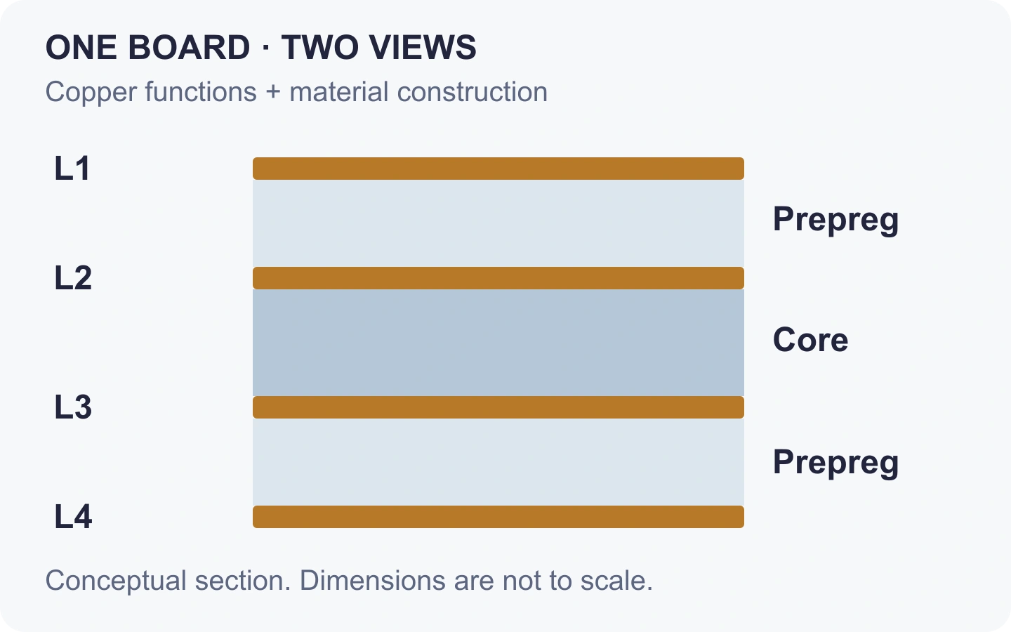
PCB Stackup
A PCB stackup describes how copper and insulating layers are arranged. Review layer order, core and prepreg descriptions, and thickness when preparing a multilayer board.
Controlled Impedance
Controlled impedance depends on the conductor geometry, dielectric properties and reference structure. The guide explains why trace dimensions and stackup are reviewed together.
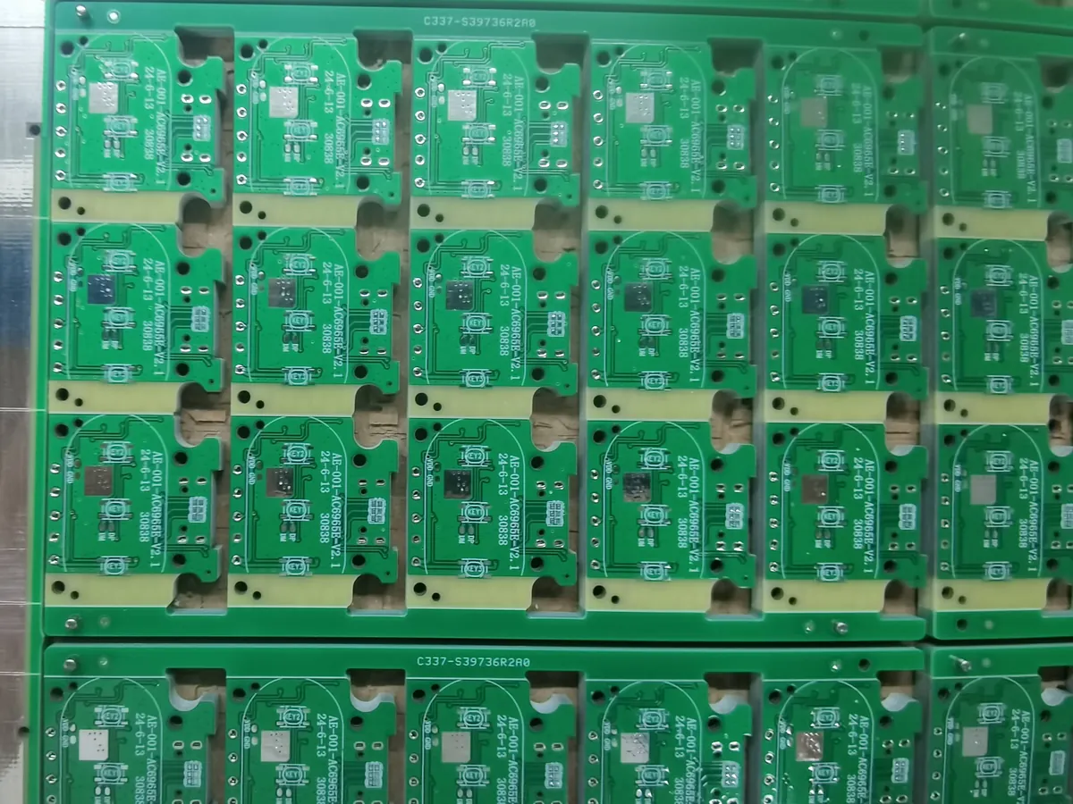
Panelization groups boards for manufacturing and assembly.
PCB Panel Requirements
Panelization helps boards move through assembly and separation. Review board shape, process rails, spacing and the choice between V-scoring and routed breakaway tabs.
PCB Materials and Surface Finishes
The base material and surface finish serve different purposes. The substrate is part of the board structure and affects electrical, thermal and mechanical behavior. Surface finish protects exposed copper and supports the intended soldering or contact requirements.
PCB Raw Materials
Learn about common substrate materials and the characteristics to consider when selecting a board construction.
PCB Surface Finishing
Compare surface treatment methods, including HASL and ENIG, and consider how the choice relates to the assembly process and the finished board.
PCB Fabrication and Assembly Processes
PCB fabrication produces the bare board; PCB assembly adds and solders components to that board. Each stage uses different project information and introduces different manufacturing considerations.
PCB Manufacturing Process
Follow the main stages of bare-board fabrication, from manufacturing data and materials through drilling, patterning, finishing and inspection.
PCB Assembly Process
See how fabrication data, component information and assembly instructions connect with paste printing, placement, soldering and inspection.
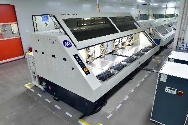
Fabrication and assembly involve different production stages.
BGA Assembly
BGA solder joints sit beneath the package, so pad and via design, assembly conditions and inspection access deserve particular attention.
PCB Inspection, Testing and Quality
Different tests answer different questions. Choose a method based on the object being checked, the features that are accessible and the result your project requires.
| Bare-board PCB testing | PCB assembly testing | |
|---|---|---|
| What is checked | The fabricated board before components are installed | The board after components have been assembled |
| Examples | Visual or optical checks and electrical tests for opens and shorts | Assembly inspection, electrical checks and functional tests |
| Starting point | PCB Test | Assembly Testing |
An electrical pass on a bare board does not establish that an assembled product performs its intended functions. Similarly, a functional test checks the functions and conditions defined by its procedure; it does not automatically inspect every solder joint.
Quality Assurance
Learn how quality considerations connect materials, fabrication, inspection and assembly.
Where Should You Start?
Choosing board construction? Start with PCB Stackup and PCB Raw Materials.
Preparing an impedance-controlled design? Review Impedance Control alongside the stackup.
Planning a build? Explore the manufacturing process, assembly process and panel requirements.
Defining inspection or tests? Start with PCB Test for the bare board, or Assembly Testing for the assembled board.
Review Our Manufacturing and Assembly Capabilities
These resources explain design and process topics. To review GreatPCB’s published specifications for rigid, flex, metal-core and SMT projects, visit our PCB Manufacturing and Assembly Capabilities page and follow the relevant detailed table.
Discuss Your PCB Project
Share your Gerber files, stackup, quantities and any special manufacturing or test requirements. For assembly, include the BOM and placement information so we can understand the complete project scope.