SMT vs SMD: Key Differences in Components and PCB Assembly
In engineering documents, SMT and SMD are two terms that are often confused. A buyer may ask, “Can you do SMT?” while an engineer may say, “This SMD package is difficult to solder.”
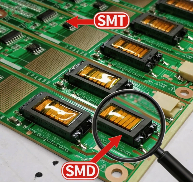
What is the difference between SMT and SMD? The answer is simple: SMD means Surface Mount Device, while SMT means Surface Mount Technology. The former is the component on the BOM, while the latter is the manufacturing process used to mount and reliably solder the component to the PCB.
What often causes project delays is not a lack of understanding of the definitions, but confusion about the roles of the two:
- The design team specifies an SMD package but does not provide clear requirements for pads, stencil design, and placement tolerances.
- The purchasing team only specifies SMT assembly but does not clearly define inspection, reflow, and component supply risks.
- The manufacturing team discovers only after reviewing the files that 0402, BGA, QFN, or high-frequency components need additional process control.
So, this article does more than explain the basic concepts. It explains from an engineering perspective how SMD affects manufacturability, how SMT affects solder joint reliability, and how to distinguish the two during component selection, DFM, quotation, and acceptance.
1. First, What Is the Difference Between SMT and SMD?
In one sentence:
SMD is “what component is used,” while SMT is “how the component is mounted and soldered to the PCB.”
| Dimension | SMD | SMT |
|---|---|---|
| Full Name | Surface Mount Device | Surface Mount Technology |
| Nature | Component package or device | PCB assembly process |
| Main Focus | Component size, leads, terminals, package, MSL, and supply method | Solder paste printing, placement, reflow, inspection, and rework |
| Typical Output | Resistors, capacitors, ICs, BGA, QFN, connectors, and other BOM items | PCBA manufacturing process, SMT line, process window, and inspection standards |
| Main Responsibility | Component selection, supply chain, and package library | PCB design, manufacturing engineering, SMT assembly, and quality inspection |
| Common Failure Sources | Incoming component defects, poor lead coplanarity, and poor moisture control | Poor solder paste printing, placement shift, incorrect reflow profile, voids, and solder bridges |
Therefore, SMD is the object, while SMT is the method.
You can choose a 0402 capacitor, and that is an SMD. But mounting it consistently on a PCB and forming a reliable solder joint requires a complete SMT process.
2. What Is an SMD? It Is More Than Just a “Small Component”
2.1 The Core Definition of SMD
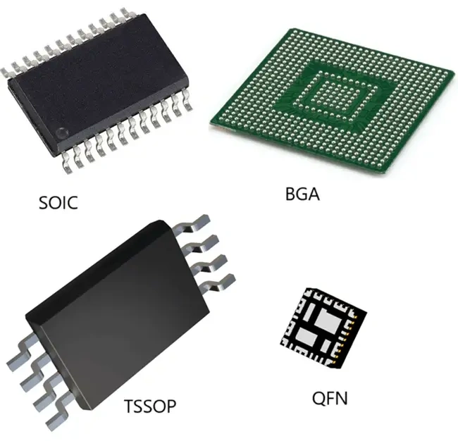
SMD refers to electronic components designed for surface mounting. Unlike traditional through-hole components, SMDs usually do not have long leads that pass through PCB holes. Instead, they are soldered directly to pads on the PCB surface through terminals or solder balls.
Common SMD types include:
- Passive components: Resistors, capacitors, and inductors, such as 0402, 0201, and 01005 packages.
- Semiconductor packages: SOT, SOP, TSSOP, QFP, QFN, and DFN.
- Bottom-terminal components: BGA, LGA, and QFN.
- Structural parts and connectors: SMD connectors, EMI shields, test points, and USB connectors.
For high-density PCBA, the value of an SMD is not only its small size. It also provides shorter interconnection paths, lower parasitic inductance, and a structure that is well suited for automated assembly.
2.2 SMD Parameters That Really Affect Solderability
Many engineers focus only on package size, but the production line pays close attention to several other details:
- Terminal material and plating: Whether the surface can wet properly and whether it is suitable for lead-free soldering.
- Lead coplanarity: Warped leads on QFP and QFN packages can directly cause soldering defects.
- Package height: This affects placement force, thermal behavior during reflow, and rework space.
- Moisture Sensitivity Level (MSL): Components with higher MSL requirements can suffer internal damage during reflow when their floor life is exceeded.
- Pad and stencil matching: Pads that are too large can increase tombstoning risk, while pads that are too small can cause insufficient solder.
- Thermal mass: Large pads, thick copper areas, and small-lead components can respond differently to the same reflow profile, which may result in uneven heating.
Therefore, SMD selection should not be based only on the package drawing in the datasheet. You also need to consider whether the component fits your SMT process window.
3. What Is SMT? A Process System That Turns SMDs into Reliable Solder Joints
3.1 The Core Definition of SMT
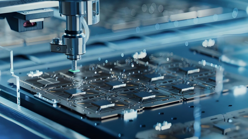
SMT stands for Surface Mount Technology. It is not a single operation. It is a complete manufacturing process used to assemble SMDs onto a PCB and create reliable electrical connections.
A typical SMT process includes:
- PCB incoming inspection: Check pads, solder mask, surface finish, and board warpage.
- Solder paste printing: Print solder paste onto the pads through a stencil.
- SPI: Inspect solder paste volume, height, offset, and insufficient solder.
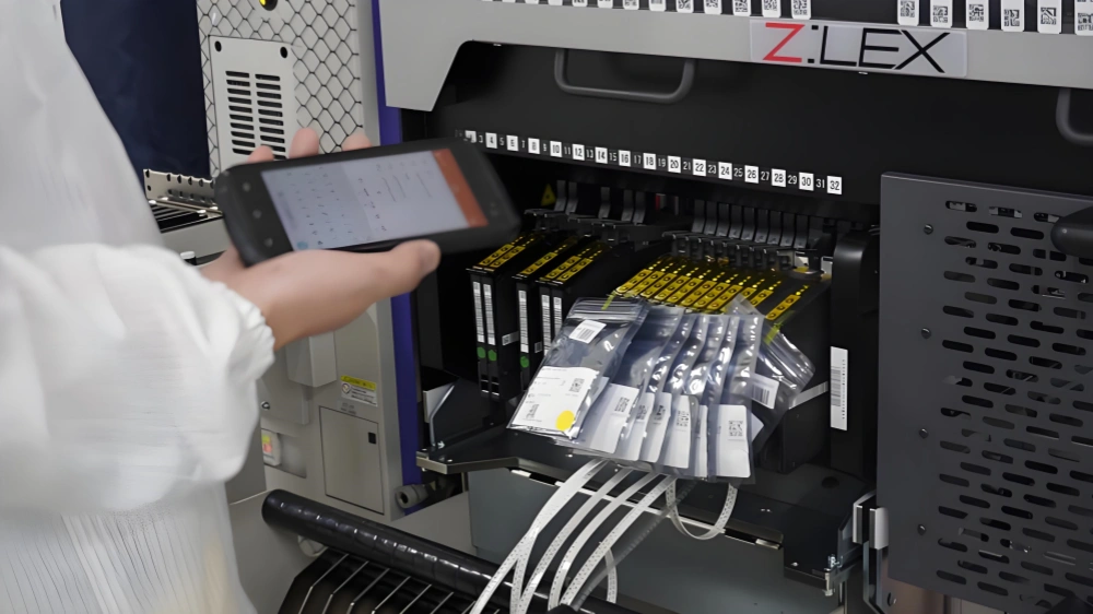
- SMD placement: Use a pick-and-place machine to place components at the specified coordinates.
- Reflow soldering: Heat the PCB through controlled temperature zones so the solder paste melts and forms solder joints.
- AOI: Check component presence, wrong components, polarity, tombstoning, solder bridges, and other visible defects.
- X-ray inspection: Check hidden solder joints, especially for BGA and QFN packages.
- Rework and touch-up: Repair defective solder joints or components.
- Post-assembly processes: Cleaning, conformal coating, final assembly, functional testing, and other processes.
3.2 A Key SMT Process: Solder Paste Printing Often Determines Much of the Quality
In PCB factories, a common view is that a large share of SMT defects can come from solder paste printing.
Solder paste printing depends on several variables:
- Stencil thickness: Affects solder paste volume.
- Aperture design: Affects paste release and solder bridge risk.
- Squeegee pressure and speed: Affect printing consistency.
- Stencil release speed: Affects the shape of the printed solder paste.
- Pad cleanliness: Affects solder wetting.
For fine-pitch ICs, BGA, and QFN packages, too much solder paste can cause bridging, while too little solder paste can cause opens.
This is why precision SMT manufacturing often uses automated solder paste inspection systems, such as configurations used for industrial PCBA.
3.3 Placement and Reflow: It Is Not Simply “Put It on the PCB and Heat It”
During placement, key factors include:
- Placement accuracy: Especially important for 0402, 0201, and 01005 components.
- Nozzle selection: Helps prevent component damage and placement shift.
- Feeder stability: Feeder vibration can increase pickup failures and misplacement.
- Coordinates and rotation angles: Incorrect polarity or orientation can directly cause functional failure.
During reflow, the process must control:
- Preheat ramp rate: Helps prevent thermal shock.
- Soak zone: Allows the flux in the solder paste to activate properly.
- Peak temperature: Must meet the wetting requirements of the solder alloy.
- Cooling rate: Affects solder joint structure and thermal stress.
- Temperature uniformity: Large boards, thick-copper boards, and mixed-load boards are especially sensitive.
When the same PCBA contains both a large thermal-mass connector and a 01005 resistor, the reflow profile must meet the needs of both.
Otherwise, a large component may not wet properly while a small component may become overheated or tombstone.
4. The Real Relationship Between SMD and SMT: The Component Sets the Limits, While the Process Determines Yield
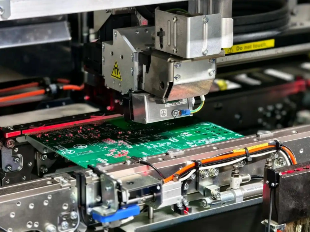
Many project problems look like “SMT defects” on the surface, but the root cause is often a mismatch between the SMD and the SMT process.
4.1 SMD Package Characteristics Can Limit the SMT Process Window
| SMD Feature | Impact on SMT | Engineering Response |
|---|---|---|
| 01005, 0201, and other small packages | High requirements for printing and placement accuracy | Use high-precision placement and AOI inspection |
| BGA and LGA bottom-side solder joints | Solder joints are hidden | Use X-ray inspection for soldering quality |
| Large QFN thermal pad | Risk of insufficient solder or voids under the center pad | Use segmented stencil apertures and control solder volume |
| High thermal-mass components | Slow heating during reflow | Optimize the reflow profile and use zone-based control when needed |
| Fine lead pitch | Higher risk of solder bridges | Control stencil thickness, aperture design, and PCB pad design |
| Moisture-sensitive components | Risk of internal damage during reflow | Strictly control MSL, baking, and floor life |
4.2 SMT Capability Also Determines Whether an SMD Can Be Used Properly
Selecting a high-performance SMD is only the first step. The second step is whether the manufacturing process can assemble it consistently.
For example:
- You choose small passive components. Does the assembly line have the required placement accuracy and AOI capability?
- You choose BGA or QFN. Does the factory have X-ray inspection for voids, shift, and solder defects?
- You choose a high-density multilayer PCB. Does the factory have stable solder paste printing and reflow control?
- You choose a high-frequency RF module. Does the manufacturer understand the effects of pads, impedance, and reflow on signal integrity?
This is why SMT in a complex PCBA project cannot be understood simply as “placing components.”
It is the combined result of materials, equipment, process parameters, inspection, and engineering experience.
5. How Should SMT and SMD Be Distinguished in BOM, DFM, and Purchasing?
5.1 In the BOM: SMD Is a Component Attribute
In a BOM, engineers normally describe the SMD itself:
- Package: 0402, 0603, SOT-23, QFN, BGA
- Component value: 10 kΩ, 100 nF, 3.3 V LDO
- Brand and MPN
- Packaging method: Tape and reel, tray, or tube
- Moisture sensitivity level and storage requirements
The key point is:
The BOM describes the component, not the manufacturing process.
5.2 In DFM: SMD Must Match the SMT Pads, Stencil, and Inspection Process
During DFM review, SMD and SMT should be evaluated together:
- Are the PCB pads matched to the component terminals?
- Is the solder mask web sufficient?
- Does the stencil aperture need to be reduced, expanded, or segmented?
- Is there enough spacing for AOI and rework?
- Are polarity markings clear?
- Are test points accessible?
- Does the high-density area require local panelization or process rails?
If DFM only checks whether the PCB can be routed, but does not check whether the PCB can be assembled consistently, problems often appear during the pilot run.
5.3 In Purchasing: SMT Refers to the Manufacturing Service Scope
When buyers request “SMT assembly,” they often need to clarify:
- Single-sided or double-sided assembly
- Whether PCB fabrication is included
- Whether component sourcing is included
- Whether the board contains BGA, QFN, 01005, or other difficult-to-place components
- Whether AOI, X-ray, and SPI are required
- Whether reflow profiles, inspection images, or first article approval are required
- Whether conformal coating, cleaning, aging, or functional testing is required
So, it is correct for purchasing to ask about SMT and for engineering to discuss SMD. The key is to define both within the same project context.
6. In High-Frequency, Automotive, and Complex PCBA Applications, How Do SMT and SMD Differences Affect Reliability?
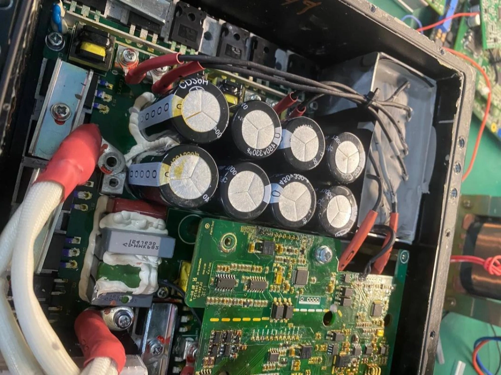
6.1 High-Frequency Projects: SMD Packages and SMT Soldering Both Affect Signal Quality
In 5 GHz, Wi-Fi, millimeter-wave front-end, and communication module projects, an SMD is not just a package choice. It can also affect parasitic parameters, current return paths, and impedance continuity.
For example, matching capacitors, inductors, filters, and connectors in an RF path can introduce additional parasitic inductance and impedance discontinuity when the pad design is not correct or the solder joint shape becomes inconsistent after reflow.
For high-frequency projects, PCB stack-up, return paths, via stitching, pad dimensions, and component packages should be considered together.
In some 5 GHz or higher-frequency PCBA projects, the manufacturer needs to do more than place SMD components. It also needs to understand the requirements of high-frequency signals for solder joints, pads, and assembly consistency.
For example, services such as High-Frequency 5GHz SMT PCB Assembly show why SMT and SMD need to be evaluated together.
6.2 Automotive Electronics: Wide Temperature Ranges Increase the Impact of SMT Solder Joint Defects
Automotive electronics often operate across wide temperature ranges, such as -40°C to 125°C, with some applications requiring even higher temperatures.
In these environments, the difference between SMD and SMT can directly affect solder joint life.
Common risks include:
- Solder joint fatigue caused by thermal cycling
- Insufficient reflow for components with different thermal masses
- Narrower soldering windows on thick-copper boards
- Crack growth in solder joints under vibration
- Internal component damage caused by poor moisture control
Therefore, wide-temperature PCBA should not be evaluated only by whether the components were successfully placed.
Solder wetting, voiding, component stress, and process consistency must also be considered.
For projects involving -40°C to 125°C or -40°C to 150°C operating conditions, the SMT process should carefully evaluate materials, components, and the reflow process window.
6.3 High-Density Boards: Smaller SMDs Require Stronger Inspection Capability
As PCBAs move toward multilayer boards, HDI structures, and fine-pitch components, the SMT challenge changes from “Can we place the component?” to “Can we place and inspect it consistently?”
For example:
- 01005 and 0402 components require higher placement consistency.
- BGA and QFN hidden solder joints require X-ray inspection to support quality evaluation.
- Precision PCBAs with tolerances around 0.1 mm require higher manufacturing and inspection capability.
- 8-layer and higher-density SMD PCBAs are more sensitive to warpage, thermal mass, and reflow uniformity.
At this stage, SMT is not simply a collection of machines. It is a system that combines stencil printing, placement, reflow, AOI, X-ray, and engineering experience.
7. Common Misunderstandings: Why Are SMT and SMD Often Confused?
Misunderstanding 1: Treating SMD as a Manufacturing Capability
“We need to do SMD.”
This can be understood in casual conversation, but it is not precise enough for formal engineering documents.
SMD is a component type. What should actually be defined is the SMT process capability, inspection standard, and acceptance criteria.
Misunderstanding 2: Making SMT Responsible for Every Problem
A soldering defect is not always the SMT factory’s fault.
Poor lead coplanarity, failed moisture control, or incorrect PCB pad design can all be root causes. Even a strong SMT process can only reduce the risk. It cannot remove a problem that starts with the component or design.
Misunderstanding 3: Looking Only at Package Size
A 0402 capacitor may look small, but if the pads are not balanced or the stencil apertures are too large, tombstoning can occur.
A BGA may be an advanced package, but if the stencil design for the center thermal pad is not correct, insufficient solder or excessive voiding can occur.
Misunderstanding 4: Ignoring Inspection Capability
For visible solder joints, AOI can detect common defects such as component shift, solder bridges, tombstoning, and insufficient solder.
For hidden solder joints such as BGA and QFN, visual inspection or AOI alone is often not enough. X-ray inspection may be required to evaluate the internal solder joints.
8. From SMD to Reliable PCBA: Why the Manufacturing Partner Matters
Once you understand the difference between SMT and SMD, the real challenge is turning this knowledge into stable mass production.
This requires a manufacturing partner that understands the boundary between the two.
The manufacturer should be able to evaluate pad design, stencil design, and placement difficulty based on the SMD package, while also controlling solder paste printing, placement, reflow, and inspection from the SMT process side.
This is where GreatPCB has an advantage.
For high-frequency and complex PCBA applications, GreatPCB's service pages cover 5 GHz, 5G-ready, and 10 GHz advanced PCB design, as well as 5 GHz SMT/SMD PCB Assembly, Turnkey PCB Assembly, and Rapid PCB Assembly.
This means the project can be evaluated beyond simple component placement, with high-frequency signals, component packages, and assembly processes considered together.
For industrial and automotive electronics, the related capabilities cover wide-temperature PCBA applications such as -40°C to 125°C and -40°C to 150°C, as well as SMT/SMD PCB Assembly, Rigid PCB ODM, and double-sided boards with 35 μm copper.
These projects test more than individual equipment. They require a complete understanding of thermal cycling, thick-copper heat transfer, and solder joint reliability.
For precision placement and inspection, GreatPCB provides automated SMT lines, AOI inspection, and X-ray inspection, and supports applications involving 01005 component placement, 0402 BGA PCBA ODM, 0.1 mm tolerance PCBA, 8-layer SMD PCBA, and 8-head SMT PCBA.
For small-size, high-density, and bottom-terminal components, this closed loop of placement + inspection + engineering feedback is a key factor in reducing pilot-run risk.
When a project is no longer simply asking, “What do SMT and SMD mean?” but needs to turn SMD components into a stable and deliverable PCBA, the engineering capability of the manufacturing partner can directly affect first-pass yield and mass-production consistency.
Conclusion: SMD Defines the Component, While SMT Determines the Assembly Quality
Back to the original question: What is the difference between SMT and SMD?
- SMD is a Surface Mount Device, which belongs to the component and package side.
- SMT is Surface Mount Technology, which belongs to the manufacturing and process side.
- SMD defines the design limits, while SMT affects solder joint reliability.
- High-quality PCBA comes from the coordination of SMD selection, DFM design, SMT processing, and inspection capability.
When your project involves high-frequency signals, small-size components, BGA/QFN packages, wide-temperature environments, or complex multilayer boards, evaluating SMD and SMT together at an early stage can reduce rework, shorten the pilot-run cycle, and improve mass-production consistency.
For projects involving 5 GHz high-frequency applications, complex SMD packages, or turnkey assembly requirements, you can start with High-Frequency 5GHz Turnkey PCB Assembly to evaluate the SMT/SMD manufacturing requirements and get project-specific guidance.
Table of Contents
Related Posts
PCBA Prototype
September 8, 2026