
Why Is There Too Much Solder Paste? Stencil Thickness, Apertures and Printing Checks
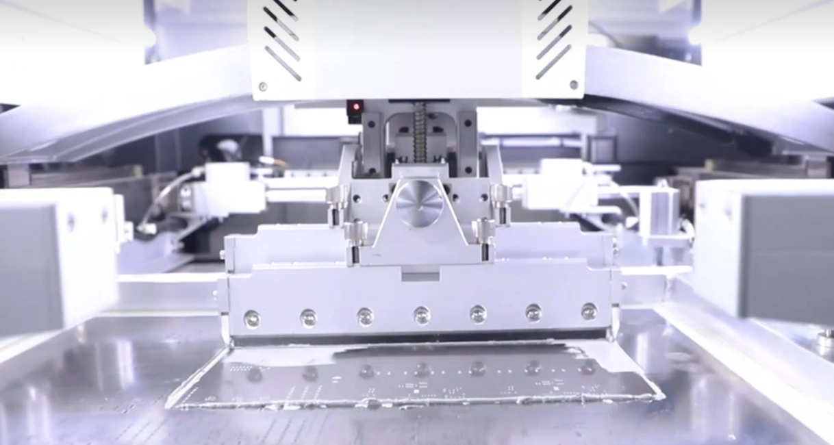
A fine-pitch connector looks clean in the PCB layout, but the first paste print tells a different story: adjacent pads appear joined by a thin smear. Is the stencil too thick? Are the openings too large? Or did the stencil move when it was lifted?
Too much solder paste can result from the stencil design, but excess-looking deposits are not always a volume problem. A shifted print, poor contact between the stencil and board, paste left on the underside of the stencil, or movement during separation can also put material where it does not belong.
Start by looking at the paste before components are placed and before reflow. Note whether the issue affects the whole board, one package type or only a few individual pads. That pattern helps narrow the investigation before anyone changes the stencil or the solder paste.
In short, use the deposit shape to distinguish paste volume from paste placement. A tall, correctly positioned deposit calls for a different check from paste smeared between pads. Measure the deposits when possible and compare them with the agreed print criteria for the assembly.
What Does the Paste Print Tell You?
The shape and distribution of the deposits provide useful clues. They do not, on their own, prove a single cause.
| What you see after printing | What to check first | Why it matters |
|---|---|---|
| Most deposits appear consistently larger or higher than intended | Stencil thickness, aperture dimensions, print setup and specified paste volume | The opening and foil thickness set the nominal space available for paste, while the print determines what reaches the board |
| Paste smears between adjacent pads | Stencil-to-board contact, alignment, board support and underside cleanliness | Paste can escape beneath the stencil or move during separation |
| The deposits are shifted in the same direction across the board | Board registration, clamping and stencil alignment | A consistent offset suggests checking the shared positioning setup |
| Fine openings print too little or inconsistently | Aperture size and wall condition, paste particle size, filling and release | Paste that remains in an opening does not reach the pad |
| A large deposit is lower in the middle | Aperture size, blade condition and printing pressure | The blade can remove material from a wide opening during the stroke |
| One print looks good, but later boards deteriorate | Cleaning interval, paste condition and changes during the print run | A blocked opening or paste on the stencil underside can change later deposits |
Compare affected and unaffected boards where possible. Record the component reference, board side and revision, stencil identification, print sequence and inspection images. A photo taken after reflow may show a bridge, but it cannot tell you by itself whether the paste was already smeared during printing.
If the paste print looks acceptable but a short appears only after reflow, investigate the later steps too. Component placement, solder wetting and the reflow process may all be relevant; an electrical short alone does not identify which step introduced the problem.
How Stencil Thickness and Apertures Affect Paste Volume
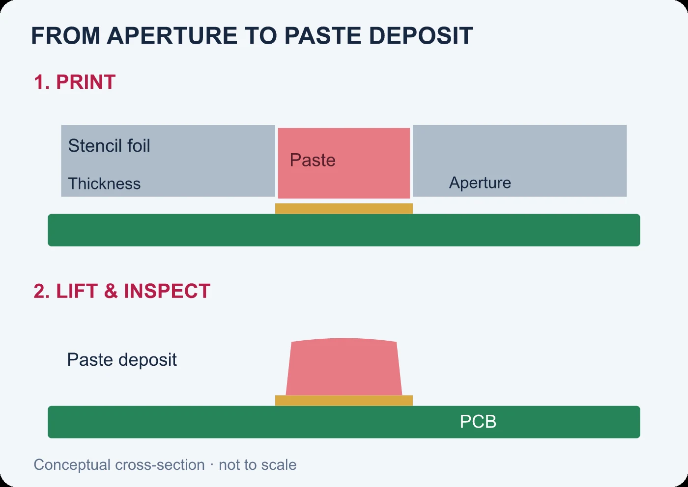
How paste moves from a stencil aperture to a PCB pad. Conceptual illustration, not to scale.
A solder paste stencil is a sheet with openings, called apertures, positioned over the areas where paste is needed. During printing, paste fills the openings. When the stencil separates, part of that paste remains on the PCB pads.
The nominal volume inside a simple straight-sided aperture is:
Aperture volume = opening area × stencil thickness
This is a useful starting point, not a measurement of the finished print. Aperture shape and wall condition, paste properties, printing setup and separation all affect how much paste actually transfers to the PCB.
A simple thickness comparison
Imagine that the aperture area and every other condition remain unchanged. Reducing the foil thickness from 0.12 mm to 0.10 mm reduces the theoretical aperture volume by approximately 16.7%:
(0.12 − 0.10) ÷ 0.12 × 100 = 16.7%
That calculation does not guarantee a 16.7% reduction in the printed deposit. In production, compare the actual deposits and assess whether the change also leaves sufficient paste for larger components.
Why one thickness is a compromise
A board can contain both fine-pitch ICs and larger power devices or connectors. Small apertures need reliable paste release; larger joints may need more solder. Reducing foil thickness for a fine-pitch package affects the whole stencil unless a stepped construction or another process is used.
Aperture geometry can be adjusted as part of the solution. Some boards may benefit from a step stencil with areas of different thickness, but it is not automatically necessary for every mixed layout. Component requirements, print equipment, stencil construction and cost should be reviewed together.
Small Apertures: Why Paste Can Stay in the Stencil
Paste must release from the aperture walls as the stencil lifts. If an opening is very small relative to its depth, release can become less consistent. This is why stencil design often considers the area ratio: the area of the aperture opening compared with the area of its walls.
How to Calculate the Area Ratio
For a rectangular aperture with straight walls, one way to express it is:
Area ratio = (length × width) ÷ [2 × (length + width) × thickness]
Use the same units for all three dimensions. A smaller ratio can make paste release harder, but a ratio alone does not establish the outcome: stencil manufacturing, wall finish, paste and printer settings also matter.
A Worked Example
For a worked example, a rectangular opening that is 0.30 mm long and 0.25 mm wide in a 0.10 mm thick stencil has an area ratio of approximately 0.68:
(0.30 × 0.25) ÷ [2 × (0.30 + 0.25) × 0.10] ≈ 0.68
These dimensions illustrate the calculation; they are not a recommended aperture for a particular component. Compare the result with guidance for the stencil process and package, and verify the actual print. A passing calculation does not by itself guarantee a sound solder joint.
For example, STMicroelectronics’ LGA assembly guidance discusses area ratio, foil thickness and paste inspection for its LGA package guidance. Its values and recommendations should be read with that package and process context, not treated as a promise for every design.
If small pads print too little while larger pads look normal, review the affected aperture geometry and paste release before assuming the entire stencil must be made thinner. Check for blocked apertures and printing conditions at the same time.
Check the Paste Layer Alongside the PCB Design
The copper pad, solder mask opening and paste aperture describe different things. The copper pad forms the board-side soldering surface. The solder mask defines exposed areas around the copper. The paste layer defines the intended stencil openings.
Those shapes may look similar in a layout tool, but they are not interchangeable. An aperture may be reduced, divided into several openings or omitted for a particular build. A design file should make the intended board side and revision clear so the stencil is not made from an outdated or unintended layer.
Do not-populate positions
If a component is marked DNP or DNI, decide how its paste opening should be handled for that product variant. Printing paste on an unpopulated position can leave unwanted solder deposits after reflow; keeping an opening can also affect how a shared stencil is managed across variants.
Make the decision with the assembly team rather than assuming the BOM alone will alter the stencil. Identify variant-specific DNP positions in the released files, and confirm which paste data will be used for each build. Our PCB BOM guide explains how fit status and material information work together.
QFN exposed pads and window openings
Large exposed pads can need a different paste pattern from the smaller signal pads around them. Dividing one large opening into a group of smaller windows is one approach to managing the paste deposit. It can also help address uneven printing across a large opening.
The geometry must suit the exact package, pad, thermal-via arrangement and assembly process. Freescale’s Chinese-language PQFN application note AN2467 discusses stencil design for its PQFN package family; use the actual component documentation and manufacturing review for the project at hand.
An open via in a pad can also affect where molten solder goes during reflow. Stencil design does not replace a decision about the via construction. See our via-in-pad guide and QFN soldering guide for those related questions.
If the Apertures Look Right, Check the Printing Setup
A stencil can match the released paste file and still produce a poor print. The board, stencil, paste and printer have to work together.
Alignment and board support
The stencil must register with the board and remain in position during the print. Check the board orientation, fiducials where used, clamps and support beneath the PCB. A thin or unevenly supported board may not contact the stencil consistently over its whole area.
If every deposit is offset in the same direction, check the common alignment setup first. If the problem appears only near an unsupported area or board edge, review local contact and support as well.
Paste under the stencil and blocked openings
Paste on the underside of the stencil can transfer outside the intended aperture pattern. Material left in apertures can cause low or missing deposits on later boards. Inspect both sides of the stencil and use a cleaning plan suited to the paste, stencil and production run.
Look for a trend: a clean first print followed by worsening deposits suggests a different investigation from a consistent defect on every print. Cleaning frequency is process-specific; an arbitrary interval is not a substitute for observing the results.
Solder paste inspection, or SPI, can measure deposit position, area, height and volume where the equipment and inspection program support those measurements. Compare results across pads and boards to identify a pattern, then check the stencil, board support or printing setup suggested by that pattern. Our solder paste inspection guide explains the inspection stage in more detail.
Squeegee, paste and separation
Blade pressure and speed influence how paste fills the openings. Too much pressure can remove paste from large openings or affect contact; too little can leave openings incompletely filled. During separation, movement between the stencil and PCB can distort the deposit.
Paste storage, conditioning and usable life also affect printing. Follow the paste manufacturer’s instructions for the material in use rather than applying one storage or warming time to every product.
What to Review with Your Assembly Partner
A useful conversation starts with the exact build package and a description of the observed print. Before changing a stencil, share:
- Board and assembly revision: Identify the PCB version, populated variant, board side and any DNP positions.
- Component requirements: Flag fine-pitch parts, large thermal pads, unusual connectors and the applicable package recommendations.
- Paste data: Provide the intended top and bottom paste layers when available, together with notes about custom aperture patterns.
- Responsibility for changes: Agree whether the assembler may adjust apertures during CAM preparation and how proposed changes are reviewed.
- Inspection evidence: Identify which positions need first-print review and whether photos, measurements or a solder paste inspection report are required.
For an existing issue, include photographs taken immediately after printing and identify whether the same defect appears on every board or develops during the run. That information can make the discussion more useful than sending a post-reflow photo alone.
GreatPCB supports PCB assembly projects from prototypes to production. Share the build files, component packages and any known printing concerns so the assembly scope and inspection requirements can be reviewed with the project.
Frequently Asked Questions
Should every stencil aperture be smaller than the PCB pad?
No. The required opening depends on the component, pad, stencil thickness and process. Some apertures are reduced, some are divided into windows, and others may follow the pad geometry. Check the component manufacturer’s guidance and the intended assembly process.
Is a thinner stencil always better for fine-pitch parts?
Not always. A thinner foil can reduce nominal paste volume and may help with some small apertures, but it also changes the deposit for other components on the board. Evaluate the complete component mix and actual print results.
Can too much solder paste cause solder bridging?
Yes. Excess paste can contribute to a bridge, especially where soldering areas are close together. However, a bridge can also involve alignment, smearing, component placement or reflow conditions. Inspecting the print before placement helps narrow the cause. See how to prevent solder bridging for a broader discussion.
Should I remove paste openings for components that are not fitted?
The intended paste pattern should match the build variant. If a stencil will be shared between variants, discuss the DNP positions and stencil strategy with the assembler before ordering or printing.
Who changes the stencil apertures: the designer or the assembler?
Either may propose a change, depending on the project. The important step is to identify the released paste data, agree on who can modify it and communicate the approved pattern. Review a proposed change against the component and board requirements before it is used in production.
Table of Contents
Tags
Related Posts
PCBA Prototype
November 4, 2026
PCBA Prototype
November 3, 2026

PCBA Prototype
October 30, 2026