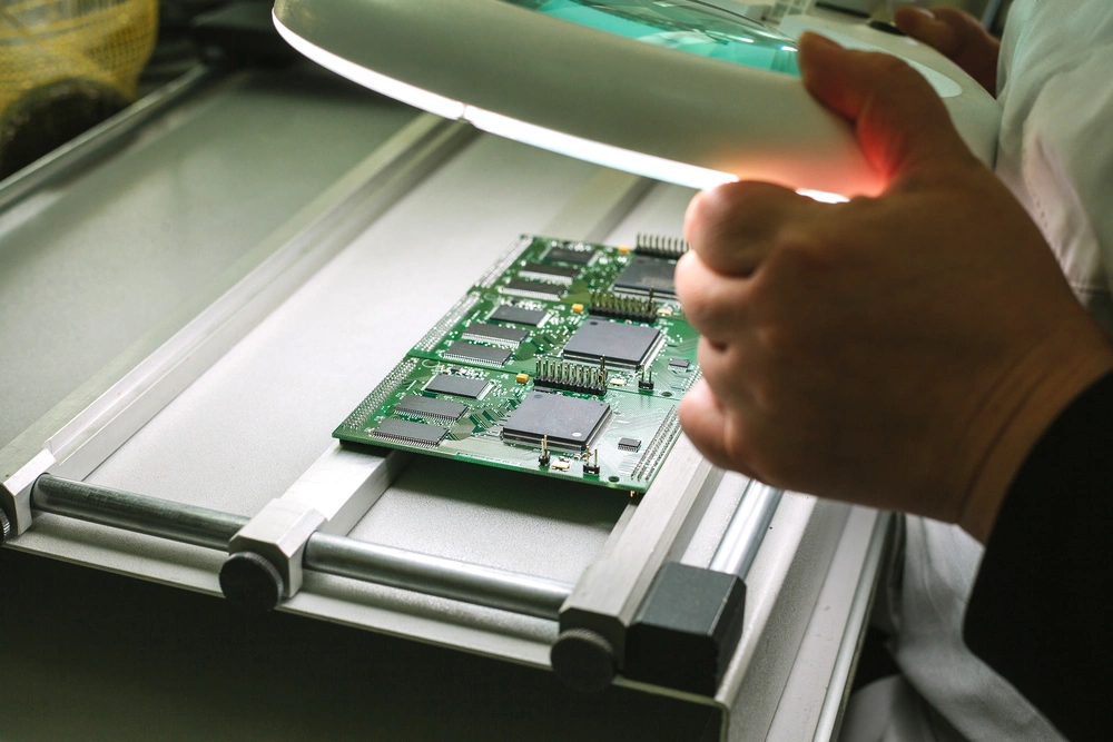
PCB Assembly Receiving Inspection: What to Check When Your Boards Arrive
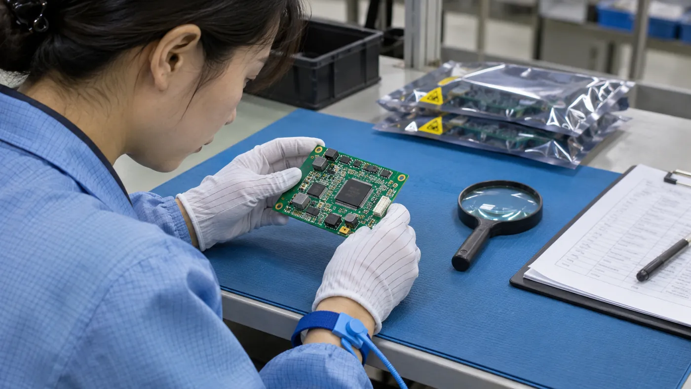
Your assembled boards have arrived. The box looks intact, the supplier’s report says “pass,” and the boards appear ready to use. Before installing or powering them, take a few minutes to confirm that the shipment matches the order and that the required inspection and test records belong to the correct boards.
A PCB assembly receiving inspection starts with the delivery, revision and quantity; continues with a visual check of the accessible board and components; and ends with a decision to release, hold or investigate the material. The depth of the check depends on the product, the order and the quality plan agreed with the manufacturer.
This guide covers assembled boards received from a supplier, rather than incoming inspection of bare PCBs or loose components before assembly.
Start with the Shipment and Packaging
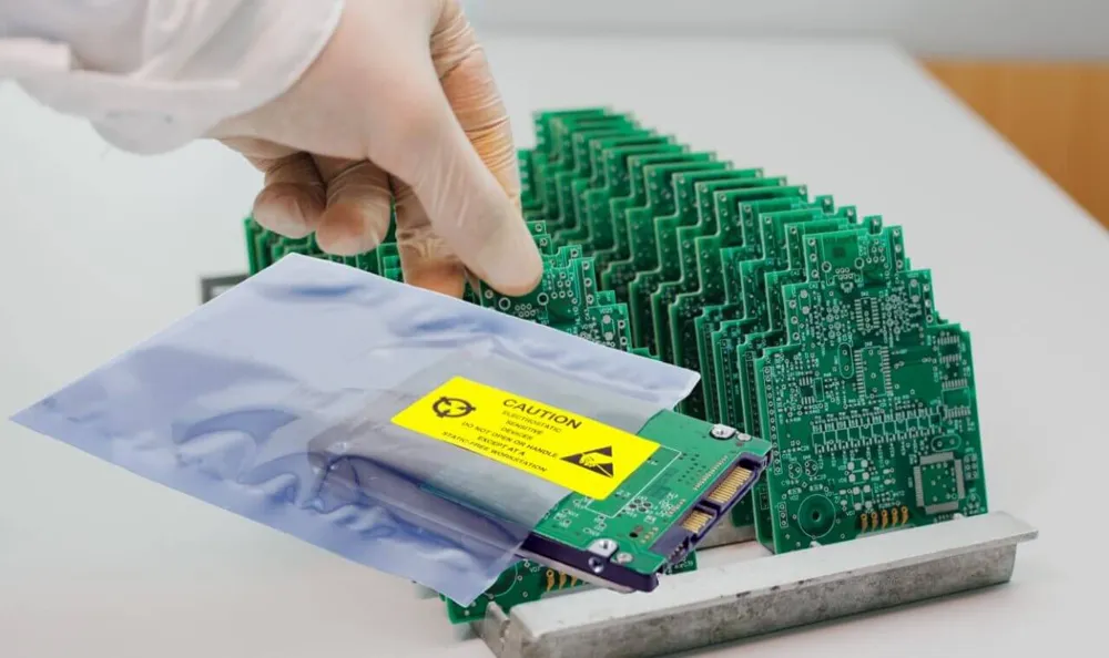
Check the carton count against the shipping documents and photograph visible transport damage before removing or repacking the contents. Keep the packaging and labels with the shipment if there is a discrepancy.
Count the delivered assemblies and distinguish completed boards from spare parts, bare boards or separately packed accessories. If the order was split into multiple shipments, compare the delivered quantity with the packing list for that shipment, not just the overall purchase order.
Handle electrostatic-discharge-sensitive assemblies according to your ESD control procedure. Open protective packaging in an appropriate protected area, and retain the original labels and bags when boards need to be held for investigation.
Identify the lot before mixing boards
Record the purchase order, supplier, delivery date, board part number and revision. Where the project uses serial or lot numbers, keep them associated with the inspection results. Mixing boards from different deliveries before recording their identity makes it harder to determine which units are affected by a later finding.
Confirm the Board Revision and Assembly Variant
An assembly may have the correct board outline but the wrong component population or firmware. Compare the delivered boards with the released documents for that order: the assembly drawing, BOM, approved changes and any variant-specific instructions.
| Check | Compare with | What a mismatch may mean |
|---|---|---|
| Board part number and revision | Purchase order and released PCB drawing | The wrong revision was shipped, or the identification needs clarification |
| Component population | Approved BOM and assembly drawing | A component may be missing, substituted or intentionally not fitted |
| Labels and serial numbers | Project identification requirements | A label may be missing, duplicated or assigned to the wrong unit |
| Firmware and programming | Agreed firmware version and programming record | The version or programming status needs verification |
| Approved deviations | Written approval and affected board range | A permitted change may apply only to certain boards or quantities |
An empty location is not always a missing part
A footprint with no component can be a do not populate (DNP) position. Before treating it as a defect, check the reference designator against the approved BOM and the specific product variant. A photograph or the PCB silkscreen alone may not show whether that location was intended to be fitted.
Similarly, a component with a different visible marking is not automatically incorrect. Check the approved manufacturer part number and any documented alternatives. If a marking is unreadable or the substitution is unclear, ask the supplier for the relevant identification records rather than guessing from the package color or size.
Inspect Accessible Features Before Powering On
Use suitable lighting and magnification for the features you need to inspect. Avoid placing unnecessary pressure on small components, connectors or solder joints. Compare questionable areas with the approved drawing or another board from the same configuration.
Set up the inspection and photographs
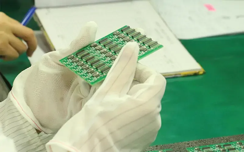
Start with an overall view of both sides of the board, then work through the components, connectors and accessible solder joints in a consistent order. Use even lighting and change the viewing angle when reflections obscure a feature. Select magnification that makes the feature visible while leaving enough surrounding area to understand its location.
For a questionable feature, photograph the whole board and then take a clear close-up. Include the reference designator where possible, and associate the images with the board’s serial or lot number. Handle the assembly using the project’s ESD precautions; avoid touching exposed contacts or cleaning an area before it has been documented.
Look for physical damage and contamination
Check board edges, connectors and taller components for cracks, bent pins, loose parts or obvious impact damage. Look for foreign material and unusual residue in accessible areas. Photograph the observation before cleaning: residue may be acceptable or unacceptable depending on the materials and agreed requirements, and appearance alone does not establish its electrical effect.
Check that connectors and mechanical parts appear correctly seated and match the assembly drawing. A damaged connector can prevent a test fixture from making reliable contact even if the board itself is otherwise functional.
Examine the board edges and corners for cracks or damage that could have occurred during depanelization, handling or shipment. An apparent bend should be assessed against the drawing and agreed requirements; a visual impression alone does not establish whether the board is outside a specified flatness limit.
Check visible components and solder joints
Compare component locations and polarity marks with the released assembly drawing. Look for clearly displaced components, visible solder bridges, detached leads or other obvious damage. Where the product uses a workmanship standard or customer-specific acceptance criteria, use the agreed class and revision to assess the finding.
Do not decide that every irregular-looking joint is defective based on appearance alone. Record the location and request a review against the applicable criteria. Hidden joints beneath BGA and other bottom-terminated packages cannot be assessed fully by looking at the top of the component.
Common findings and what to check next
| What you see | Check before reaching a conclusion | Practical next step |
|---|---|---|
| An empty component position | The BOM, assembly drawing, variant and do-not-populate instructions | Record the reference designator and resolve any document mismatch |
| Bent connector pins or a cracked housing | The drawing, the packaging and other boards from the same delivery | Photograph the condition and hold affected boards for review |
| A possible solder bridge between visible leads | The location, intended connections and applicable acceptance criteria | Record the finding; use electrical verification if needed to establish the network condition |
| Residue or loose material | The agreed cleanliness requirement and whether the material is loose or part of the process | Photograph the area and agree on inspection or cleaning before altering it |
| A jumper wire or hand modification | The approved engineering change, deviation and affected serial or lot numbers | Confirm the modification is authorized for that board and revision |
These are observations to investigate, not automatic pass-or-fail rules. Use the order’s drawings, acceptance criteria and documented approvals to make the disposition decision.
What Can a Receiving Inspection Actually Prove?
Different checks answer different questions. A visual check can reveal a damaged connector, but it cannot establish that every hidden connection is sound or that the product meets its functional requirements.
| Check or record | What it can address | What it does not establish on its own |
|---|---|---|
| Visual inspection | Accessible components, labels, visible damage and solder features | Hidden solder connections or powered circuit behavior |
| AOI results | Features covered by the approved optical inspection program | Every hidden joint or every possible electrical failure |
| X-ray inspection | Internal or concealed features visible under the chosen inspection method | Complete circuit function or long-term product reliability |
| Bare-board electrical test | Opens and shorts within the specified bare-board test scope | Correct assembly, firmware or powered operation |
| Functional test | Specified behavior under the documented inputs and limits | Every operating mode, environmental condition or lifetime requirement |
For more detail on how these methods differ, see our PCB assembly testing and inspection guide. The checks performed for an order depend on what was specified and agreed.
When an inspection result does not answer the whole question
An AOI pass covers the visible features and conditions included in the inspection program; it does not establish the condition of every concealed joint. For a BGA or another package with hidden contacts, review whether the agreed plan calls for X-ray or a different verification method. X-ray can provide information about hidden structures, but it does not demonstrate that the circuit performs its intended function.
Similarly, a functional-test pass applies to the documented inputs, outputs and limits used during that test. If the application depends on a particular interface, load or firmware version, check whether it was included in the reported test before assuming that it was verified.
Read the Test Report Alongside the Actual Boards
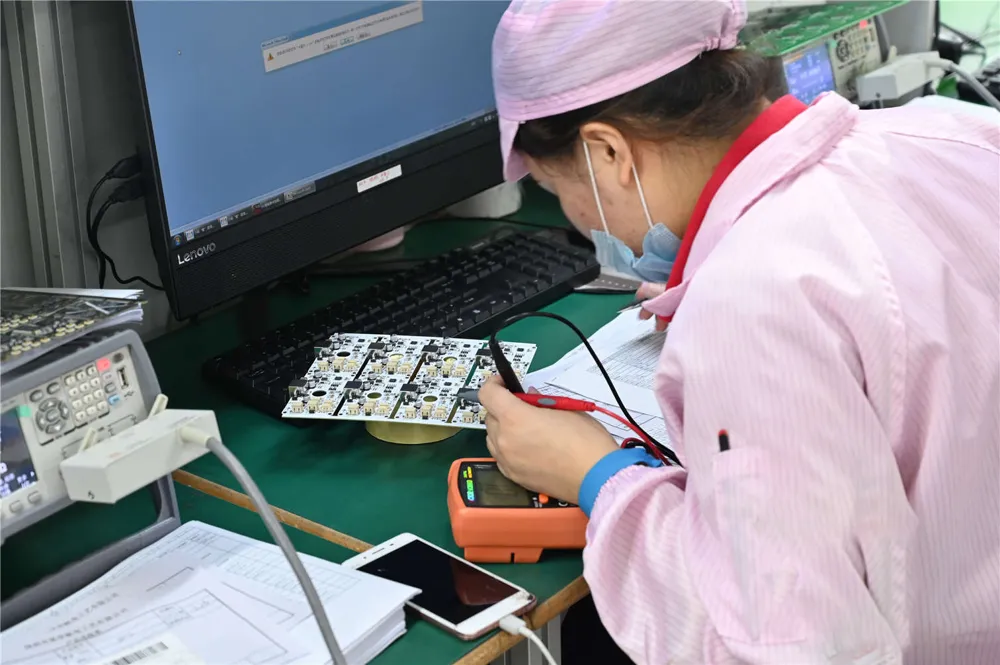
“Test passed” is useful only when the report identifies what was tested. Check the report against the order and, where applicable, the delivered serial numbers or lot:
- Identity: board part number, hardware revision and product variant.
- Coverage: test method, selected functions and any sampling or exclusions.
- Configuration: firmware or test-program revision where relevant.
- Results: the recorded result, applicable limits and any approved deviations or retests.
If the report refers to a different revision, or a required record is missing, hold the affected boards while the discrepancy is resolved. The issue may be a documentation error rather than a physical defect, but it should be clarified before the boards are released for use.
Prepare for the First Power-On
Before applying power, confirm the board identity, connector pinout, input polarity, approved supply voltage and the intended test procedure. Use the power source and current limits appropriate to the design, and connect any required load or interface as specified by the responsible engineer.
If a board has visible damage, a suspected short, an unknown modification or unclear wiring, resolve the concern before power-on. A controlled test protects the board and makes the result easier to interpret.
Watch for unexpected current draw, heat, smell or other abnormal behavior, and stop the test if it is unsafe or outside the agreed limits. A board that starts successfully has passed that particular startup check; it has not necessarily passed communications, load, environmental or long-duration testing.
For a new product moving toward a larger build, our PCB pilot build guide explains how to review wider production readiness.
What to Do When a Board Fails Inspection
Separate the observation from the diagnosis
An unpopulated position, a nonresponsive interface or an unusual current reading is an observation. Its cause may involve the board, component, firmware, test setup or a mismatch between the delivered variant and the documents used for inspection.
Keep affected units identified and separate from released stock. Depending on the potential scope, the hold may need to cover more than one board until the team understands whether the finding is isolated.
Send the supplier a useful discrepancy report
Include the information needed to locate and reproduce the issue:
- Purchase order, delivery date, board part number and revision.
- Affected quantity, serial or lot numbers and the total quantity received.
- Reference designator or physical location, with clear overview and close-up photos.
- The expected condition and the observed condition.
- The test setup, supply, firmware and measured result when the problem occurred during testing.
- Relevant BOM, drawing, approved change or test report revision.
For example, a receiving team might report: Controller board, Rev B; connector J3; two pins appear bent; two of 20 boards affected. The record can include a board overview, a connector close-up, the relevant serial numbers and photographs of any damaged packaging. The affected boards remain identified while the supplier reviews the observation and the applicable requirements.
Agree on the next step with the supplier: it may be a document correction, additional inspection, return, replacement or authorized rework. Avoid cleaning, removing components or altering a suspect board before the investigation plan is agreed, unless a safety or containment procedure requires otherwise.
PCB Assembly Receiving Inspection Checklist
| Step | Check | If something does not match |
|---|---|---|
| Shipment | Cartons, labels, quantity and visible transport damage | Record the discrepancy and retain packaging |
| Identity | Board number, revision, variant and lot | Separate affected material and verify the released order |
| Population | BOM, DNP positions, polarity and approved substitutions | Identify the reference and compare the current assembly documents |
| Condition | Connectors, board edges, components and visible joints | Photograph the finding and check agreed acceptance criteria |
| Records | Inspection, test, firmware and deviation documents required by the order | Confirm that each record applies to the delivered configuration |
| Power-on | Supply, pinout, test setup and expected response | Stop if unsafe; document the setup and measured behavior |
| Disposition | Released, held and investigated quantities | Obtain the appropriate approval before using held material |
Choose inspection coverage and sampling according to the project risk and the agreed quality plan. A short receiving check is useful, but it should not replace the production inspection or functional testing required by the order.
Frequently Asked Questions
Should every board be inspected?
The appropriate coverage depends on the purchase agreement, product risk and the checks being performed. Some projects require individual checks; others use an agreed sampling plan. Specify the plan and acceptance criteria before delivery.
Does an empty component footprint mean the assembly is defective?
Not necessarily. It may be an intentional DNP location or part of another product variant. Compare it with the approved BOM and assembly drawing before raising a missing-component issue.
Can I rely on AOI instead of functional testing?
AOI checks features visible to the configured optical system. Functional testing applies defined inputs and checks the board’s responses. They answer different questions and may be used together when the project requires both.
What if the test report says pass but the board does not work?
Check that the report matches the board and revision, then compare the reported test scope with the failing function. Record the firmware, connections, supply and observed result, and share them with the manufacturer for investigation.
Should I repair a damaged board before contacting the supplier?
First follow your safety and quality procedures. When practical, photograph and identify the condition and agree on the investigation or rework plan before changing the board, so useful evidence is retained.
Plan Inspection Before Your Next Build
The most useful receiving check starts before the order ships. Share the released BOM and assembly drawings, identify the required inspection and functional checks, and agree on the records and acceptance criteria for the project.
GreatPCB supports PCB assembly projects from prototypes to production. Discuss your board, quantity and testing requirements with our team through PCB assembly services or contact GreatPCB.
Table of Contents
- Amata i le Felauaiga ma le Afifiina
- Fa'amaonia le Toe Teuteuga o le Komiti Fa'afoe ma le Suiga o le Fonotaga
- Siaki Mea e Mauaina A'o Le'i Fa'agaoioia le Malosiaga
- O le ā moni lava e mafai ona fa'amaonia e se Su'esu'ega o le Taliaina o Tagata?
- Faitau le Lipoti o Su'ega Fa'atasi ma Laupapa Moni
- Sauniuni mo le Uluai Fa'agaoioiga o le Malosiaga
- Le Mea e Fai Pe a Lē Manuia se Su'esu'ega a le Komiti Fa'afoe
- Lisi Siaki o le Su'esu'ega o le Fa'apotopotoga PCB
- Fesili e Masani ona Fesiligia
- Siakiina o le Fuafuaga A'o Le'i Fausia Lau Galuega e Sosoo Ai
Tags
Related Posts
PCBA Prototype
November 11, 2026
PCBA Prototype
September 8, 2026