


Build a circuit that fits the product, rather than designing the product around separate circuit boards and cables. A rigid-flex PCB combines rigid component areas and flexible interconnections in one construction, giving your team more freedom to arrange electronics across multiple planes.
GreatPCB provides rigid-flex PCB fabrication and assembly for prototypes and production projects. Share your board files, stackup and mechanical requirements with us to discuss the construction, inspection and quantity for your build.
Rigid-Flex Design & Manufacturing Guide
Explore stackup, bending, fabrication and assembly in our 13-page technical guide. PDF review copy; diagrams are illustrative.
What Is a Rigid-Flex PCB?
A rigid-flex PCB integrates rigid board sections and flexible circuit layers into a single interconnected board. The rigid areas provide stable locations for components, connectors and mounting features. Flexible layers continue between the rigid sections and can be formed to fit the enclosure.
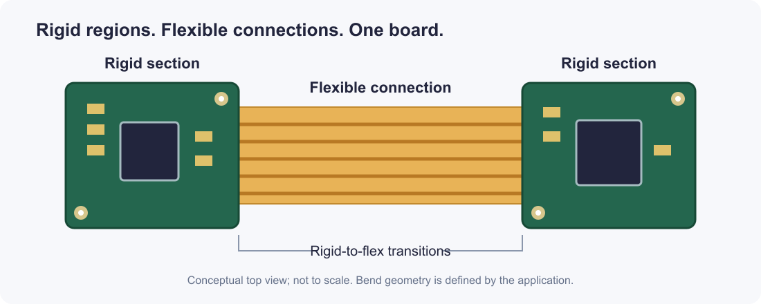
Rigid-flex construction: flexible circuitry connects rigid sections in one board. Conceptual illustration, not to scale.
Unlike a cable soldered or plugged between separate boards, the flexible connection is part of the PCB construction. A plated interconnection in a rigid area can connect the flex circuitry to other layers, depending on the stackup. The finished design is manufactured flat and then formed into its required shape during installation.
Rigid-flex is also different from a flexible PCB with a stiffener. A stiffener adds mechanical support to a flexible circuit, such as underneath a connector. In a rigid-flex construction, the rigid areas contain circuit layers that are integrated electrically and mechanically with the flex layers.
| Construction | How the sections connect | When it is useful |
|---|---|---|
| Rigid boards and cable | Separate boards are linked by a cable or connector | Modules must be detached, replaced or positioned farther apart |
| Flex PCB with stiffener | A flexible circuit receives local mechanical reinforcement | A flexible connection needs support at selected components or contacts |
| Rigid-flex PCB | Rigid and flexible circuit layers form one integrated construction | Components and interconnections must fit into a compact three-dimensional space |
Why Use a Rigid-Flex Circuit Board?
Fit electronics into a smaller assembly
Flexible sections allow rigid component areas to sit on different planes or wrap around parts of an enclosure. This can help designers use space around displays, batteries, sensors and mechanical mounting points that would otherwise be difficult to reach with a flat board.
Reduce separate interconnections
When a flexible circuit connects rigid sections directly, some board-to-board connectors and cable assemblies may no longer be needed. Fewer separate parts can simplify the bill of materials and installation sequence. The design still needs appropriate mechanical support and an agreed inspection plan.
Consider the complete system cost
Rigid-flex boards generally require more complex materials, tooling and fabrication steps than a comparable rigid PCB. Their value should be assessed against the complete assembly: separate connectors, cables, assembly work, enclosure space and the need to service individual modules. The most economical choice depends on the construction and production quantity.
Rigid-Flex Materials and Stackup
A rigid-flex stackup brings together materials with different electrical and mechanical roles. The arrangement should support the circuit in its flat manufacturing condition and in the shape it will take inside the product.
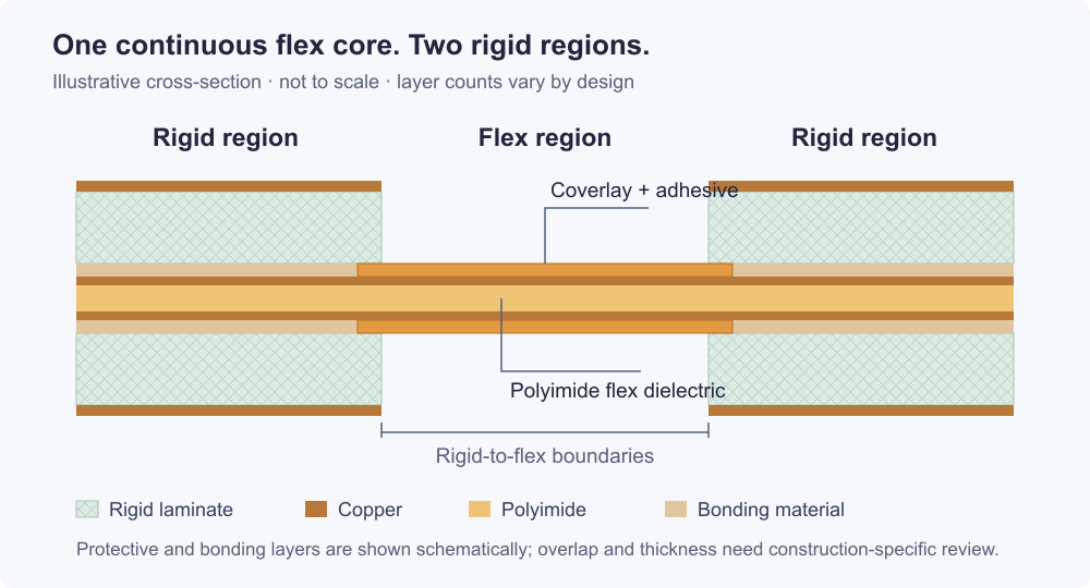
Illustrative layer arrangement. The actual stackup depends on the project.
Rigid and flexible materials
Rigid sections commonly use glass-reinforced laminate to support components and multilayer routing. Flexible sections often use polyimide-based dielectric layers with copper conductors. Depending on the design, a polyimide coverlay and adhesive protect the flexible circuitry while leaving selected pads or contact areas exposed.
The material grade and thickness influence electrical performance, thermal behaviour and bending. Copper construction matters as well: a flexible area designed for repeated movement needs its copper thickness, foil type, bend geometry and expected service cycles considered together.
An adhesiveless flexible copper-clad laminate removes a separate adhesive layer between the copper and the flexible dielectric. It does not necessarily mean the entire rigid-flex board is adhesive-free: coverlay and other bonding interfaces can still contain adhesive. Show these interfaces in the stackup so that material thickness, flexibility and processing are considered as a complete construction.
| Stackup element | Main purpose | Information to define |
|---|---|---|
| Rigid laminate | Supports components and rigid-area circuitry | Material grade, layer sequence and finished thickness |
| Flex dielectric | Supports the circuit through the flexible area | Material, thickness, layer count and bend requirements |
| Copper layers | Carry power and signals through the rigid and flex regions | Copper requirements, layer continuation and routing |
| Coverlay or flexible protection | Protects selected flexible-area circuitry | Material, opening locations and transition boundaries |
| Bonding materials | Join the construction where required | Stackup arrangement and rigid-to-flex interface |
| Surface finish | Protects exposed copper and supports assembly or contacts | Finish selection and locations requiring exposure |
Plan the rigid and flex regions together
The flexible layers can be positioned differently within the complete board construction. Some designs use flexible layers near an outer face; others integrate them between rigid-area layers. The right choice depends on routing, component locations, bend conditions, electrical requirements and the manufacturing sequence.
Show which copper and dielectric layers continue into each flexible region, where rigid materials terminate, and the intended thickness in both areas. For impedance-controlled signals, identify the trace geometry and reference structure through the rigid area, flexible section and transition. A change in dielectric thickness or reference layer can affect the electrical path.
Rigid-Flex PCB Manufacturing Capabilities
GreatPCB supports rigid-flex PCB fabrication for projects with different constructions, from early prototypes to production. Our published flex PCB capability table lists rigid-flex constructions from 2 to 18 layers and a final thickness range of 0.06 to 4.0 mm. The table does not distinguish separate thickness limits for rigid and flexible regions, so identify both on your drawing for review.
The same capability table lists materials including PI and FR-4, copper thicknesses from 1/3 oz to 2 oz, and trace/space and hole information for flex fabrication. The suitability of individual values depends on how they are combined in the complete construction. For example, copper weight, conductor geometry, flex layer count and bending requirements should be assessed together.
| Requirement | What to specify for your project | What we review |
|---|---|---|
| Board construction | Total layers, rigid and flex regions, and the layers connecting them | Layer sequence and fabrication approach |
| Thickness | Target thickness in the rigid and flexible areas | Material selection, tolerances and bend requirements |
| Copper and circuitry | Copper requirements by layer, minimum trace and spacing | Combination of copper weight, geometry and board construction |
| Holes and vias | Hole sizes, plated/non-plated features and any special via treatment | Stackup compatibility, interconnection and inspection requirements |
| Materials and finish | Material grade, coverlay and required surface finish | Availability and suitability for the specified design |
| Electrical requirements | Controlled-impedance targets, reference layers and test requirements | Stackup geometry, testing and documentation needs |
| Quantity and delivery | Prototype or production quantity, panel format and target date | Production plan, material availability and requested checks |
Review the complete flex PCB capabilities and share the design files when a project combines several demanding features.
Design for Rigid-Flex PCB Manufacturing
Define how the board will bend
Start with the installed shape. A section that bends once during installation has different requirements from a circuit designed to move repeatedly during operation. State the inside bend radius, direction, available clearance and expected movement. If the circuit will flex repeatedly, include the expected cycle count and test conditions.
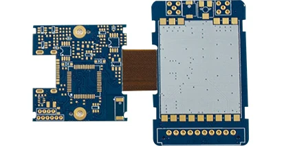
Third-party board example showing rigid sections and a flexible connection.
The thickness used to assess a bend is the thickness of the complete flexible construction at that location, not the thickness of the rigid island. Copper, dielectric, adhesive and protective layers all influence the result. For a more detailed explanation, see our rigid-flex PCB bend radius guide.
Protect the rigid-to-flex transition
The transition is where a flexible section leaves a rigid area. Because stiffness changes at this boundary, the board should have sufficient free flex length to achieve the required shape without forcing the bend directly against the rigid edge.
Identify the transition on the mechanical drawing and review nearby pads, holes, coverlay openings and copper features. Keep components and plated holes out of the active bend where practical. Smooth flex outlines and well-defined layer terminations help the manufacturer assess the design before fabrication.
Coverlay placement also affects the transition. Its protective film, adhesive and openings need to align with the flexible circuitry and nearby rigid-region features. Excess material extending into the intended bend can reduce the free length available for forming, while an opening that does not match the exposed pad area can complicate assembly. Define the boundaries and discuss the overlap with the fabricator for the selected stackup.
Review routing and electrical performance
Keep the conductor path through the bend straightforward, and avoid abrupt changes in trace width or direction inside the active bend. The arrangement of copper on multiple flexible layers affects both bending and electrical behaviour.
For high-speed signals, review the reference plane and return path through the flex section rather than assuming the rigid-area stackup remains unchanged. Controlled impedance may be possible, but the geometry and materials must be defined for the actual regions of the board. Our PCB stackup guide explains the relationship between conductor and dielectric layers.
Plan for assembly and handling
Rigid-flex boards may need support while solder paste is printed, components are placed and the assembly passes through reflow. Component locations, panel rails, fixtures and clearance around flexible sections should be reviewed together. If the project requires a carrier or special handling during assembly, include that requirement in the production discussion.
How Rigid-Flex PCBs Are Manufactured
The exact manufacturing sequence depends on the layer structure and materials. A typical project moves through the following stages:
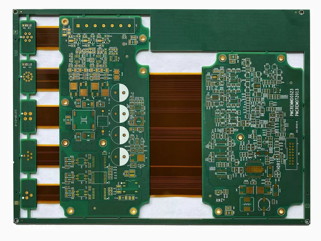
Third-party example: rigid and flexible regions arranged in a manufacturing panel.
- Design and stackup review. The fabrication data, rigid and flex boundaries, material requirements and finished dimensions are reviewed together.
- Flexible circuit preparation. Copper circuitry is formed on the flexible material, and the specified protection is applied to the appropriate areas.
- Rigid and flex integration. The flexible circuitry is combined with rigid-area materials. Alignment is important because the layers and openings must meet correctly at the transitions.
- Holes and interconnections. The required holes and plated connections are produced according to the construction, followed by the remaining circuitry and surface finish.
- Profile and inspection. The board outline and flexible sections are completed, and the finished boards are checked against the agreed electrical and dimensional requirements.
Rigid-flex fabrication requires attention to the relationship between different materials throughout these stages. A change to the stackup, hole structure or flexible outline can affect later steps, which is why an early review of the complete design is valuable.
The flexible layers can change dimensions during processing, so their artwork, coverlay openings and rigid-layer features must be planned for registration through the selected lamination sequence. Hole preparation is another important control point: drilling residue at an internal connection can interfere with later metallization, so the preparation method must be compatible with the rigid and flexible materials in the construction.
The final flexible window and board outline also need care. Removing rigid material too deeply can damage the underlying flex, while a nick or rough edge in the flexible outline can become a point where mechanical stress is concentrated. The selected profiling or release process depends on the stackup and required geometry.
Rigid-Flex PCB Assembly
You can request rigid-flex bare boards or include component assembly in the same project. GreatPCB can coordinate the PCB fabrication and assembly scope, including component sourcing, surface-mount or through-hole assembly, and inspection or testing defined for the order.
For an assembled board, provide the bill of materials, placement data and assembly drawings with the fabrication package. Identify component locations on both sides, customer-supplied parts, programming needs and any functional test procedures. Our flex PCB assembly service provides more detail on preparing flexible constructions for assembly.
Quality and Inspection
Inspection should address both the circuit and the construction. Electrical continuity and isolation checks help identify opens and shorts within the test coverage. Dimensional and visual checks can address board outlines, rigid and flex thicknesses, coverlay openings, transition areas and other specified features.
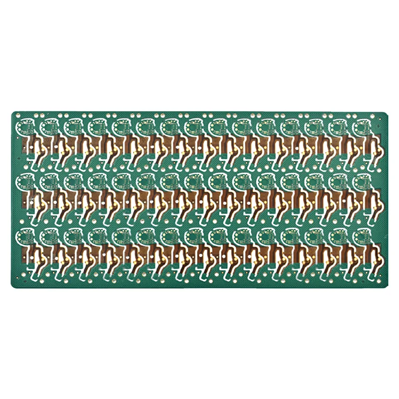
Third-party board example shown in a panel; inspection requirements depend on the project.
| Check | Purpose | Information to agree |
|---|---|---|
| Electrical continuity and isolation | Check for opens and shorts within the test coverage | Netlist and applicable acceptance requirements |
| Dimensional and visual inspection | Check specified outlines, features and visible conditions | Critical dimensions, tolerances and inspection criteria |
| Impedance verification | Assess specified controlled-impedance structures | Target values, tolerances, coupons and reporting if required |
| Assembly inspection | Check relevant placement and soldering features | AOI, X-ray or other methods appropriate to the build |
| Functional or bend qualification | Evaluate defined operation or movement | Procedure, equipment, conditions, cycle count and pass/fail criteria |
The appropriate methods depend on the project. An electrical test on a flat bare board does not by itself establish the life of a repeatedly moving flex section. When bend endurance or environmental qualification is required, define the test conditions and acceptance criteria before production.
Rigid-Flex PCB Applications
Rigid-flex construction is useful when the electrical design must follow a product’s mechanical shape.
- Medical and handheld equipment: connect circuit sections around displays, batteries and controls in a compact enclosure.
- Wearables and consumer electronics: position small rigid component areas while reducing space used by separate interconnections.
- Industrial and communications equipment: link boards located around mounting points, interfaces and mechanical structures.
- Aerospace and defense electronics: address specific packaging and interconnection requirements where the project calls for defined inspection and qualification.
The required materials, tests and documentation depend on the application and the agreed project specification.
What Affects Rigid-Flex PCB Cost and Lead Time?
The number of rigid and flex layers, materials, copper requirements, board outline and panel utilization all affect fabrication cost. Fine features, special via structures, surface finishes, inspection and qualification can add further work. Quantity also matters because engineering review, tooling and setup are distributed across the order.
The flat manufacturing outline can influence material use even when the folded product is compact. Long flex tails or irregularly arranged rigid sections may leave unused space in a panel. Reviewing the flat layout and delivery panel early can uncover alternative orientations or handling arrangements without changing the electrical function.
Lead time depends on the approved stackup, material availability, production quantity and the scope of fabrication, assembly and testing. Complete files and a clear formed-state drawing help resolve questions before a build is scheduled.
To compare design options, request quotations using the same quantity, acceptance criteria and delivery requirements. Consider the assembled product as well as the bare-board price: a design that removes connectors or reduces installation work can change the overall cost, but the result is specific to the project.
Frequently Asked Questions
Can a rigid-flex PCB bend repeatedly?
Yes, a flex section can be designed for repeated motion. The materials, copper construction, flex thickness, bend radius and expected cycles must suit the intended use. Specify the movement and qualification requirements when the stackup is reviewed.
Can GreatPCB provide rigid-flex PCB fabrication and assembly together?
Yes. Send the fabrication files along with the BOM, placement file and assembly drawing. Identify whether you will supply components and whether the project includes programming, inspection or functional testing.
What is the difference between rigid-flex and flex with stiffeners?
A stiffener reinforces selected areas of a flexible circuit. A rigid-flex PCB integrates electrically connected rigid circuit layers and flexible layers into one board construction.
Why does rigid-flex usually cost more than a rigid PCB?
Rigid-flex combines materials and manufacturing requirements for rigid and flexible regions. Layer alignment, flex protection, the outline and inspection can add work. The total product cost may also include savings from fewer separate cables, connectors or assembly steps.
Request a Rigid-Flex PCB Quote
Send your Gerber and drill files, stackup, board drawing, quantity and target delivery date. Include the flat outline and installed shape, identify the bend locations and movement requirements, and add your BOM and assembly data if components are to be fitted.
Our team will review the construction, fabrication and inspection requirements with you and prepare a quotation for your project.