
PCB Footprint Mistakes: How to Check Pinouts and Dimensions Before Ordering
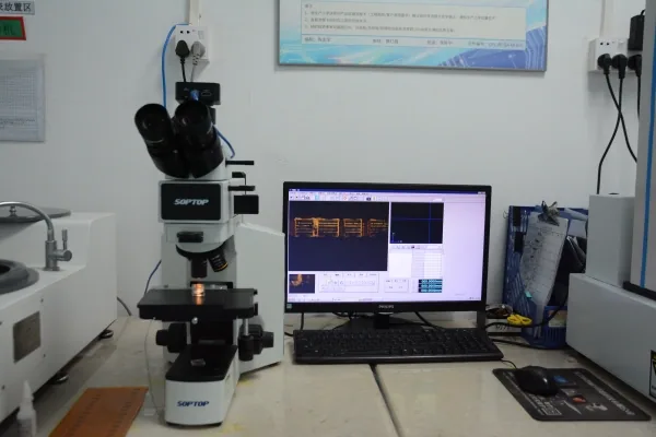
A component can fit neatly on a PCB and still be connected to the wrong signals. A connector may have its pin numbers reversed, a regulator may use a different package from the one shown in the schematic, or a mounting hole may be too small for the part that arrives.
To check a PCB footprint before ordering, start with the exact manufacturer part number. Find the package drawing that applies to that part, then compare its physical terminals with the PCB pads and the pin numbers in the schematic. Finally, review the assembly markings, clearances and exported manufacturing files.
The check is useful whether the footprint was downloaded, generated by a tool or created by your own team. A familiar library name does not establish that every pad is connected to the intended function.
What Can Go Wrong With a PCB Footprint?
In everyday PCB design, a footprint usually means the PCB representation of a component: its pads or holes, markings and other features used in layout and assembly. A land pattern describes the arrangement and dimensions of the PCB lands that connect to the component.
The schematic symbol represents electrical functions and pin numbers. The footprint locates the corresponding pads on the board. The library association connects the two. An error in any part of that chain can survive until the board is built.
| Possible problem | What you may discover | Where to start |
|---|---|---|
| Package dimensions do not match | The terminals do not align with the pads | Exact part number and package drawing |
| Pin-to-pad mapping is wrong | A signal reaches the wrong terminal | Datasheet pin table, symbol and numbered pads |
| Drawing view is misread | Connector positions or pin numbers appear reversed | Top, bottom or mating-face view in the drawing |
| Hole is unsuitable | A through-hole lead does not fit or the joint is difficult to form | Lead dimensions, finished hole and tolerances |
| Orientation mark is unclear | The assembler cannot confidently determine placement | Part marking, assembly drawing and silkscreen |
| Mechanical clearance is missed | A connector or tall component interferes with the enclosure | Component outline, height and mating space |
The first task is to establish which physical part the board is intended to receive. Then the layout can be checked against the right drawing.
Start With the Exact Part Number and Package Drawing
A product family can be offered in several packages. A suffix may identify the package, voltage option, temperature range, packing format or another feature, depending on the manufacturer. Before checking the footprint, follow the ordering information for the part listed in the BOM to the package code and drawing that apply to it.
Record the manufacturer, complete orderable part number, datasheet revision and package drawing identifier. If the part has changed or an alternative has been proposed, repeat the comparison for that alternative. A distributor listing can help locate documentation, but the final check should use the applicable manufacturer’s information.
Separate the package drawing from the recommended land pattern
The package drawing describes the component: body dimensions, terminal positions, lead sizes and tolerances. A recommended land pattern describes a suggested arrangement of copper lands on the PCB. They answer related but different questions.
For example, a lead’s width is not automatically the correct PCB pad width. The land may extend beyond the terminal to allow a solder joint to form. The recommended pattern may also depend on the assembly process or density assumptions stated in the document.
Check the units, drawing view, dimension tolerances and notes. If no recommended land pattern is provided, develop or review one with the component and assembly requirements in mind rather than assuming that the mechanical outline alone is sufficient.
One family, different pin arrangements
Texas Instruments’ LM1117 datasheet provides a useful example of why package selection matters. In its Rev. Q pin-function table, the DCY SOT-223 package assigns pin 1 to ADJ/GND, pin 3 to VIN, and pins 2 and 4 to VOUT. The NGN WSON package uses a different pin arrangement: pins 2–4 are VIN, pins 5–7 and the exposed tab are VOUT, and pin 8 is not connected.
Those assignments apply to the packages and options in that datasheet. They are not a rule for every regulator or every package with a similar name. The example shows why the BOM, package code, symbol and PCB footprint must be checked together.
Check Pin Numbers, Signals and Drawing Views
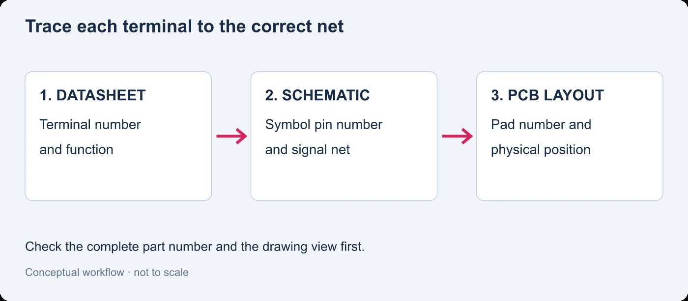
Follow terminal numbers and functions through the design. Conceptual illustration.
Find Pin 1 and identify the view
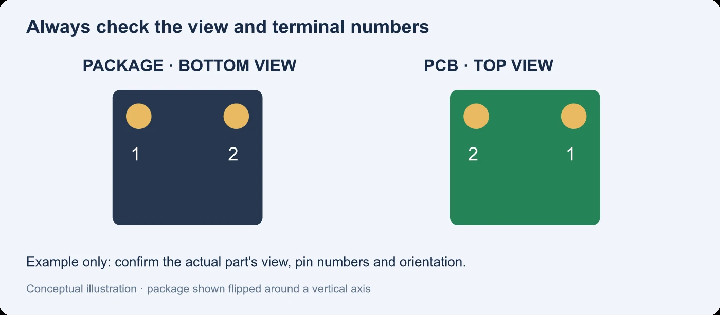
The same terminal can appear on opposite sides when the viewing direction changes. Conceptual illustration.
Start by finding the Pin 1 indicator in the manufacturer’s drawing. It may be a dot, notch, chamfer or another feature defined for that package. The PCB assembly drawing and any board marking should identify the corresponding location.
Next, look for the words top view, bottom view or another view label. A drawing of the underside of a component is observed from a different side than the top of the PCB. The positions may look mirrored, but the way to confirm the mapping is to follow the numbered terminals, not to apply an assumed flip to every package.
Connectors need particular care. A manufacturer may show the mating face, the mounting face or the component as seen from above. The connector’s keying and mechanical pins can help establish orientation, but neither replaces the drawing’s pin-number information.
Trace a pin from the schematic to the board
For each important connection, follow a complete path:
- Find the terminal number and function in the datasheet for the actual package.
- Find the same pin number and function on the schematic symbol.
- Highlight the schematic net and identify the PCB pad that carries it.
- Check that the numbered PCB pad aligns with the physical terminal in the selected package view.
- Repeat for power, ground, outputs, polarity-sensitive pins and any other critical signals.
Suppose a three-terminal device has its input assigned to terminal 3 in its datasheet. If the schematic library connects the input net to pin 1, an otherwise tidy footprint will still route that net to the wrong physical terminal. Checking the pad shape alone will not reveal the mistake.
Look beyond the first and last pin
On a display or two-row connector, it is possible for one row to match while the other is numbered in the opposite direction. Check multiple pins across both rows, especially the pins that carry power or connect to mating equipment.
For a keyed connector, check the mating part as well. The connector can be correctly placed on each board yet connect unexpected signals when the two boards are joined. Compare the manufacturers’ mating views and trace the intended connection through the pair.
Compare Pad Geometry With the Actual Component
Once the pin numbers make sense, check whether the physical terminals can be assembled onto the PCB pattern.
Pad size, pitch and spacing
Measure pad centers and compare the pitch with the recommended land pattern. Check the number of pads, their size and their position relative to the part body. On a two-row package, verify the spacing between rows as well as the pitch within each row.
Pad geometry affects more than whether the component sits over the copper. Very small lands may make alignment and joint formation difficult; oversized lands can reduce the space between adjacent solderable areas. The appropriate shape and size depend on the part and process, so do not enlarge every pad by the same amount.
Also check for differences between the component outline and the PCB courtyard. The outline describes the part’s shape or an assembly reference; the courtyard is used to manage space around it. Its purpose is not to show the electrical copper pattern.
Through-hole leads and finished holes
For a through-hole component, compare the lead’s maximum dimensions with the specified finished hole, including relevant tolerances. A square or rectangular lead needs a different clearance assessment from a round lead. Confirm whether the hole is plated and whether the datasheet shows a PCB layout or only a mechanical opening.
The drill used during fabrication is not necessarily the same diameter as the plated finished hole. Give the fabricator a clear finished-hole requirement and discuss manufacturing tolerances rather than choosing a drilling allowance from an unrelated example.
Also examine the annular ring and neighboring copper. Increasing the hole can affect the remaining pad around it and the spacing to nearby features.
Exposed pads, tabs and mechanical pins
Some packages include an exposed underside pad or a metal tab. Its electrical function is device-specific: it may connect to ground, an output or another node. The LM1117 example above shows why a tab must not automatically be assigned to ground.
Connectors may also have shield tabs, locating pegs or mounting pins. Decide which features need plated holes or solderable pads and which are mechanical openings. Then check the clearance required to insert and remove the mating connector.
For a QFN, the exposed-pad pattern, thermal vias and solder paste also affect assembly. Our QFN soldering guide explains the related soldering and inspection questions.
Check the Features Used During Assembly
Pin 1, polarity and silkscreen
The physical part, PCB layout and assembly drawing should communicate the same orientation. Check Pin 1 indicators and the polarity marks for components such as diodes, LEDs and polarized capacitors against their own datasheets.
Do not assume that a stripe or a square pad means the same electrical terminal for every part. If the component body covers the silkscreen after placement, an additional visible mark or an unambiguous assembly drawing can make inspection easier. Keep markings clear of exposed solderable areas according to the board manufacturer’s requirements.
Copper, solder mask and paste are different layers
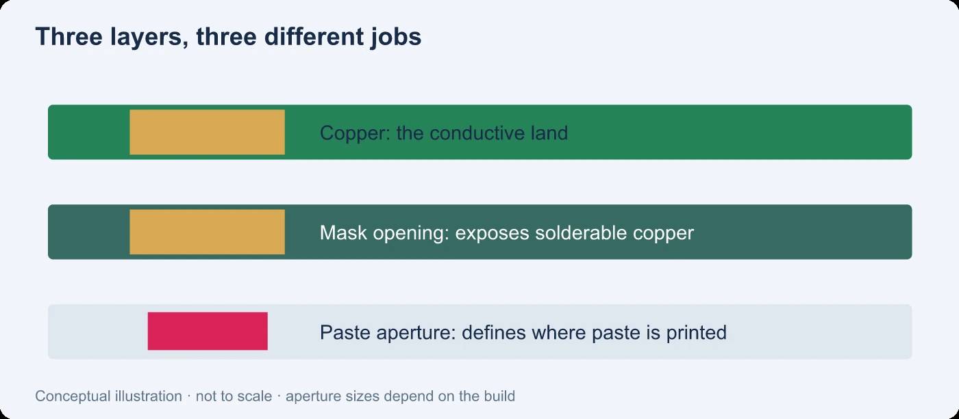
Copper, solder mask and paste each serve a different purpose. Conceptual illustration.
A copper pad provides the conductive land. The solder-mask opening exposes the area intended to be soldered. The paste layer describes stencil apertures for depositing solder paste where that process is used.
An error can occur even when the copper pattern is correct: a mask opening may expose the wrong area, or a paste aperture may not suit the pad and assembly process. Review these layers together, especially around fine-pitch parts, exposed pads and locations that should not receive paste.
Do not apply a blanket paste reduction or mask expansion to every component. Start with the component and assembler’s requirements and review the actual board construction.
Placement orientation and 3D models
Use the 3D view to look for mechanical interference, incorrect body orientation and mismatch between a model and its pads. Then verify the model itself against the actual part and enclosure. A model placed over the correct-looking pads does not prove that the pins carry the right signals.
Placement data introduces another convention: component origin, board side and rotation. Our pick-and-place file guide explains how these fields affect assembly. Confirm representative parts against the assembly drawing instead of assuming every library uses the same zero-degree orientation.
A Practical Footprint Check Before You Send the Board

A populated PCB being visually inspected under magnification.
For a new or high-risk part, keep the evidence together. The following table can be used as a review record for each reference designator or library item.
| Check | What to compare | What a pass should establish |
|---|---|---|
| Part identity | BOM manufacturer and full MPN against ordering information | The drawing belongs to the intended part and package |
| Numbering | Datasheet terminal numbers, symbol pins and PCB pads | Each selected function reaches the intended physical terminal |
| Geometry | Recommended land pattern and package drawing against the footprint | Pads or holes align with the applicable part dimensions |
| Orientation | Part marking, board mark and assembly drawing | The intended placement can be identified without relying on appearance alone |
| Mechanical fit | Body, height, mounting features, board edge and enclosure | The part has space to install and operate as intended |
| Manufacturing layers | Copper, mask, paste, silkscreen and drill outputs | The released files represent the reviewed design |
Use more than one check
Design rule checking can identify conditions covered by the rules configured in the design tool. It does not necessarily know that the library’s pin functions match the purchased part. Electrical rule checking and net highlighting are valuable, but they also depend on the correctness of the symbol and its pin definitions.
A 1:1 printout or a physical sample can help reveal an obvious mechanical mismatch. Check the printed scale before comparing the part; fine tolerances and hidden contacts still require the manufacturer’s dimensions. A 3D model helps with body and enclosure fit, provided the model and its orientation are accurate.
After making a change, regenerate the fabrication and assembly outputs. Open the exported layers in an independent viewer where practical and check representative parts, board side, drill information and markings. Make sure the BOM, assembly drawing and placement data refer to the same released revision. The PCB BOM guide covers the information needed to identify each part.
What If You Find a Footprint Error After Ordering?
The next step depends on how far the order has progressed. Identify the affected reference designators, part number and design revision before deciding on a correction.
Before fabrication begins: contact the manufacturer promptly. Correct the source design, review the affected connections and dimensions, and issue a complete replacement file set with a clear revision. Confirm which files the manufacturer will use.
After bare boards are made: assess whether the error affects mechanical fit, electrical connectivity or both. A wire modification or other controlled correction may be possible for some prototypes, while a revised board may be the practical choice in other cases. Do not assume that a physical fit means the electrical nets are safe.
After assembly: stop using the affected configuration until the circuit has been assessed. Consider the risk of incorrect power connections, component damage and rework stress. The design owner and assembly partner can review whether the boards can be reworked and how the result will be inspected or tested.
Record the correction in the component library as well as the project. Otherwise, the same footprint can reappear in the next design.
Frequently Asked Questions
Can two parts with the same package name use the same footprint?
Sometimes, but the name alone is not enough. Compare the package code, mechanical dimensions, recommended land pattern, terminal numbers and electrical functions for both exact parts. A component can fit the same copper pattern while assigning different functions to its terminals.
Is a footprint I drew myself safer than a downloaded footprint?
Either can contain an error. A downloaded footprint can save work, while a custom footprint gives the designer control over its construction. In both cases, check the completed symbol-to-pad mapping and geometry against the applicable manufacturer documentation.
If the 3D model fits, are the pins correct?
Not necessarily. A 3D model is useful for checking shape, orientation and clearance, but it may not reveal a wrong pin number or net assignment. Verify electrical mapping separately.
Will DRC catch a wrong pinout?
Not always. DRC evaluates the design against configured rules. If an incorrect library mapping is internally consistent, the design may pass those rules while connecting the wrong physical terminal. Trace the datasheet, schematic and PCB pad numbers explicitly.
Can I rotate a component to fix a wrong footprint?
Only if the corrected physical position also puts every relevant terminal on its intended pad and satisfies the mechanical and electrical requirements. Rotating a part is not a general solution for reversed pin numbering, wrong pad spacing or an incorrect library mapping.
Prepare the Design for Assembly
Footprint verification is most effective before the design is released. Match the exact part to its package drawing, trace the pin numbers through the schematic and layout, and review the mechanical and assembly details using the same board revision.
When requesting PCB assembly, provide the BOM, PCB manufacturing data, assembly drawing and placement information together. Highlight unusual connectors, exposed pads or orientation requirements so they can be reviewed as part of the build package.
Table of Contents
- What Can Go Wrong With a PCB Footprint?
- Start With the Exact Part Number and Package Drawing
- Check Pin Numbers, Signals and Drawing Views
- Compare Pad Geometry With the Actual Component
- Check the Features Used During Assembly
- A Practical Footprint Check Before You Send the Board
- What If You Find a Footprint Error After Ordering?
- Frequently Asked Questions
- Prepare the Design for Assembly
Tags
Related Posts
PCBA Prototype
November 3, 2026

PCBA Prototype
October 30, 2026
PCBA Prototype
October 30, 2026