
PCB Pad Lifting: Causes, Repair Options, and Prevention

PCB pad lifting occurs when a copper solder pad separates from the board material beneath it. The copper may remain attached to its trace, curl upward with a component lead, or tear away completely. Repairability depends on the remaining conductor, the condition of the substrate and any plated hole, and the load the repaired connection must carry.
A pad can lift while removing a component installed the wrong way round. A connector replacement can pull away both the pad and a length of trace. In either case, pause further heating and pulling long enough to inspect the damage. The next repair decision depends on which parts of the connection survived.
What Does a Lifted PCB Pad Look Like?
A solder pad is a defined area of copper where a component termination connects to the board. Its surface finish provides a solderable surface, while the underlying board material supports the copper. A lifted pad has lost some or all of that support.
Under magnification, look for a raised edge, a gap beneath the copper, or a pad moving with the component lead. If the pad has detached, the exposed area may show where it previously sat. Also examine the narrow trace leaving the pad. A small tear at that junction can interrupt the circuit even when most of the pad remains present.
Describe the condition precisely before choosing a repair.
- A partially lifted pad still has some attachment to the board, and its connecting trace may remain intact.
- A missing pad leaves an exposed area where a solderable termination is needed.
- A torn trace extends the damage beyond the pad into the circuit path.
- Damage around a plated hole or within the base material requires a wider assessment of the connection and its support.
Photographs of both sides help document the visible condition. On a multilayer board, further checks may be needed to establish the state of internal connections. Blistering or separation extending beyond the local pad also warrants investigation of the surrounding material. See the related explanation of PCB delamination.
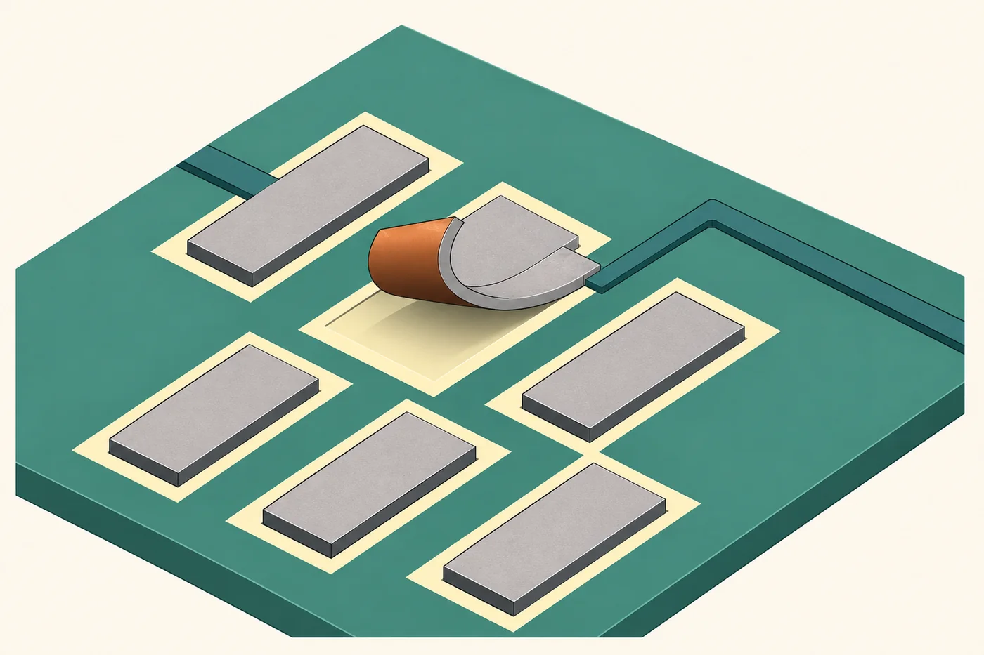
Conceptual illustration, with thickness exaggerated. The raised pad has separated from the board support while remaining attached at one end.
Why Do PCB Pads Lift During Soldering or Rework?
Heat Exposure and Repeated Rework
Thermal exposure can weaken the bond supporting the copper. Prolonged contact and repeated soldering or desoldering can contribute to damage, particularly when removal also applies force to the pad. Both the heating process and the force used to release the component belong in the investigation. Epec’s explanation of pad lifting
An iron’s displayed temperature alone gives an incomplete picture of the process. Tip size, contact quality, the solder joint, and the surrounding copper affect heat transfer. A joint connected to a large copper area can behave differently from an isolated small pad at the same tool setting.
This makes a universal repair temperature or maximum number of rework attempts difficult to apply. Review the actual thermal history and the assembly’s material and component limits. A pad that lifts during soldering provides evidence of damage, while the cause still requires investigation.
Force Applied During Removal or Handling
Pulling a component before all its soldered connections have released transfers force through the leads into the pads. A multi-pin component is particularly easy to damage this way. One remaining joint can hold the part while movement loads a small area of copper.
The same concern applies when rocking a connector, levering up a component, or trying to free a lead from a plated hole. The force may peel the pad, tear the trace, or damage the hole connection. After soldering, unsupported cables or heavy components can continue loading the repaired area during handling and use.
Board Construction and Local Support
The copper-to-substrate bond, local geometry, and mechanical support all affect how the connection responds to heat and force. Investigating repeated failures therefore requires information about the board construction and the operations performed at that location.
Record whether the problem affects one termination, one component type, or several boards from the same build. Compare the affected positions and process histories. A consistent pattern gives the fabrication and assembly teams something specific to investigate. The stage at which damage becomes visible is only one part of that evidence.
Can the Damaged Pad Be Repaired?
Check the Pad’s Electrical Role
Start by identifying what the pad connects to. A surface trace may lead to a nearby component or test point. A plated hole or via may connect it to another layer. Some component features also provide mechanical attachment.
If no trace is visible, check the schematic, layout or net information, and component pin definitions. A pad can connect to copper hidden beneath the component or inside the board. Establishing that a pin is unused requires design evidence. Its appearance in a photograph leaves that question open.
For an electrical repair, identify the intended net and an appropriate connection point. Record both before removing more copper or adding a jumper. This avoids building a repair around an assumed connection.
Inspect the Trace, Hole and Base Material
Check the trace back to sound copper and examine the material where a replacement pad would bond. Exposed fibers, missing material, or a deeply damaged surface change the repair work required. Circuit Technology Center’s epoxy pad-replacement method requires a smooth, flat bonding surface and directs technicians to address base-material damage. Epoxy-bonded surface-mount pad repair
A through-hole connection needs separate attention. An intact pad on the opposite side is useful evidence, but the hole wall and any associated layer connections still need assessment. Circuit Technology Center specifically notes that a replacement land has no intermetallic connection to the remaining plated hole. Its repair method includes additional provisions for restoring the electrical connection. Through-hole land repair
Consider Mechanical Load and Product Requirements
A small signal termination and a frequently used connector place different demands on a repair. Consider current, signal behavior, insertion and removal forces, vibration, temperature exposure, and access for inspection. These factors determine what the restored connection and its support must withstand.
The product’s repair permissions and acceptance requirements also matter. An approved production repair needs a defined method and suitable verification. Where damage is extensive, connections remain uncertain, or the required repair cannot be verified, replacing the board may be the practical decision.
| Observed condition | Information to establish | Repair assessment |
|---|---|---|
| Pad partly lifted, trace still present | Conductor integrity, remaining attachment and surrounding material | Assess whether the original copper can be retained and secured |
| Pad missing or trace torn | Intended net, sound connection point and usable bonding area | Assess replacement copper or a designed connection repair |
| Opposite-side pad looks intact | Hole-wall condition and all required layer connections | Establish whether the through-hole connection remains usable |
| Substrate damaged or connector loose | Damage depth, structural support and service loads | Assess base-material work, mechanical support and board replacement |
The table organizes the assessment. Product acceptance criteria and the selected repair procedure determine whether a particular board can return to service.
PCB Pad Repair Options and Their Limits
Securing a Partially Lifted Pad
When the original copper remains continuous and suitably positioned, retaining it may be an option under an appropriate repair procedure. The assessment must account for the condition beneath the pad and the stability of its trace connection.
Adhesive selection requires compatibility with the board, later soldering, and the product’s operating environment. Cure conditions follow the selected material and repair method. Adhesive placed beneath or around a pad provides mechanical attachment. The copper path and soldered termination require their own electrical checks.
Avoid repeatedly pressing and reheating the area while deciding what to do. Additional movement can change a partially attached pad into a missing pad and extend the damage into its trace.
Replacing a Missing Pad or Restoring a Connection
A replacement pad restores a solderable copper feature in the required position. Circuit Technology Center describes methods using liquid epoxy and pre-applied adhesive film. These methods have different bonding processes and tooling requirements. Material-specific curing or bonding instructions govern the heat, pressure, and time. Epoxy method, adhesive-film method
Where a replacement pad must reconnect to a trace, the repair includes a designed electrical joint to sound copper. Pad alignment and spacing must also suit the component. A piece of copper placed over the damaged area leaves these details unresolved until its attachment and connection are established.
A jumper wire offers another possible route for restoring a known connection. Its endpoints, conductor size, routing, insulation, and strain relief need to suit the circuit. Current-carrying requirements and signal behavior can limit where a jumper is appropriate. The repaired net should be documented so subsequent inspection can verify the intended path.
Supporting Connectors and Other Loaded Components
If a jumper allows a board to power up again, inspect how the component is held. A connector can still move and transfer insertion forces into its remaining joints or the new wire.
Mechanical provisions depend on the original assembly and the permitted modification. Mounting features, component supports, or an approved bonding arrangement may form part of the repair. Confirm clearances, mating access, and the load path before accepting the result.
For an engineering assessment, prepare clear photographs of both board sides, the component reference, available circuit information, and a description of what was removed or heated. Include the expected service conditions and any repair requirements. These details help define the scope of work before another attempt.
What Should Be Checked After a Pad Repair?
Begin with magnified inspection. Confirm pad position, conductor alignment, solder-joint condition, and clearance from neighboring features. Look for loose copper, solder bridges, damage to nearby components, and exposed areas that require protection under the repair procedure.
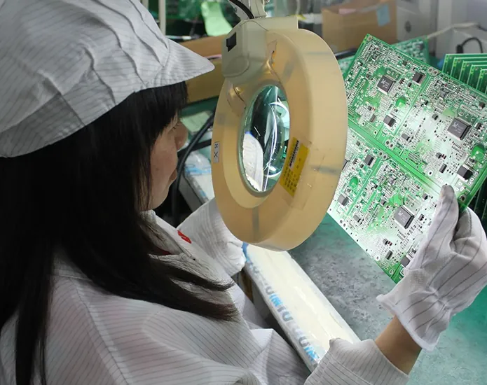
Magnified visual inspection helps examine the joint area, component position and nearby features. This photograph illustrates the inspection activity.
Then verify the repaired electrical path. Continuity testing requires a de-energized circuit and safely discharged capacitors. Follow the meter’s instructions, including its continuity threshold. A beep indicates that the measured path meets that instrument’s threshold. Fluke’s continuity-testing guidance
For a repaired capacitor pad, identify a point on the same net as that pad and test the restored conductor path between them. Measuring across the capacitor introduces the component into the measurement. Its charging behavior and other in-circuit paths can affect the reading. Choose test points from the circuit information so the measurement addresses the connection being repaired.
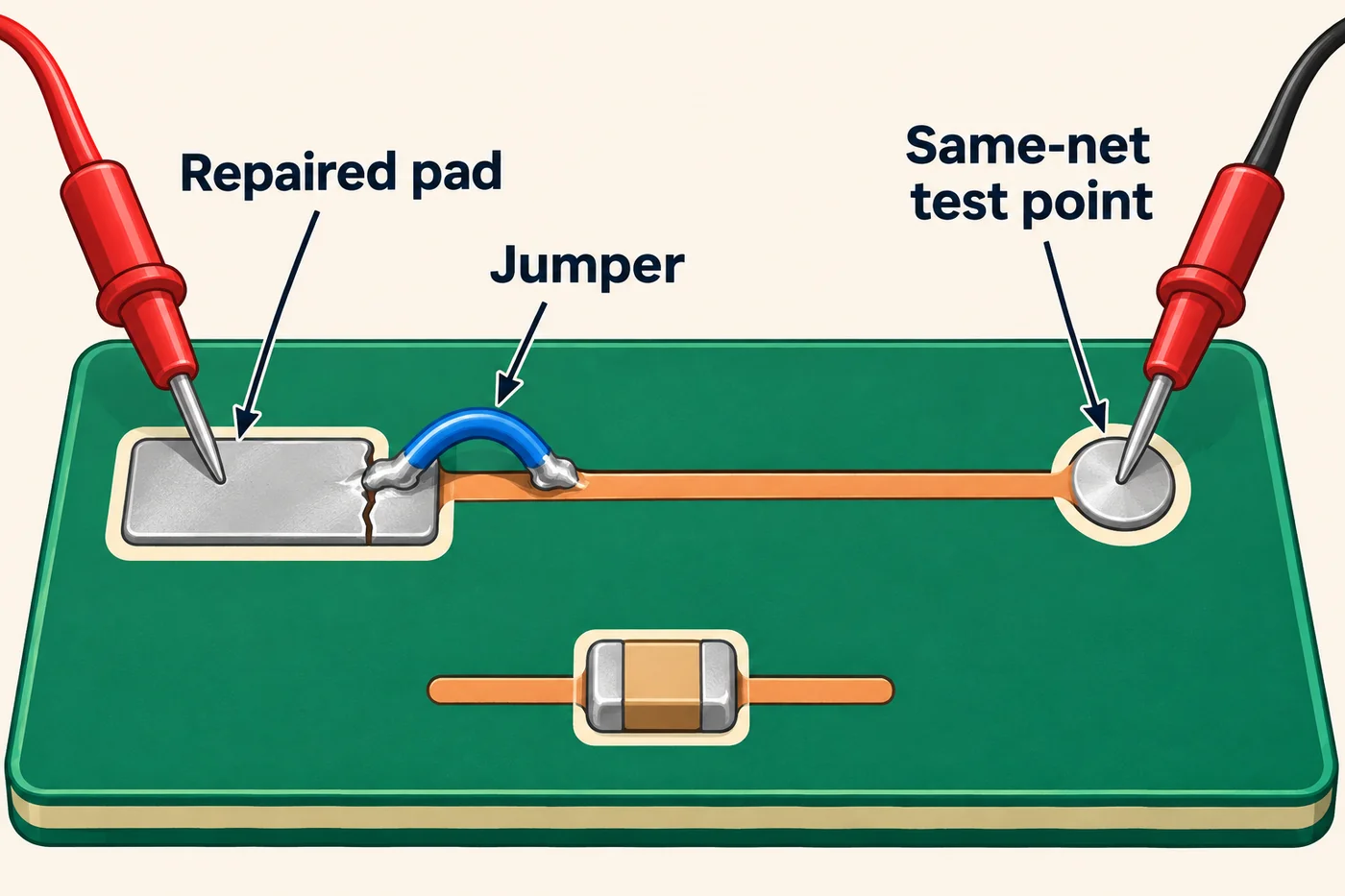
Conceptual test-point selection. The probes contact the repaired pad and a point on the same net. The separate capacitor below lies outside this test path. De-energize the circuit and safely discharge capacitors before testing.
Also check for unintended connections to neighboring nets, using the circuit’s expected behavior to interpret the results. Parallel paths can complicate in-circuit readings. An ambiguous result calls for a more suitable test arrangement.
Finally, perform the functional and other verification required for that product. Power-up is one observation in this process. The release decision should also account for the repaired connection’s electrical performance, component support, and applicable operating conditions. Keep a record of the location, repair method, and inspection and test results.
How to Prevent Pad Lifting in Future Builds
Before removing a component, establish how each termination will be released. Match the tool and tip to the joint and provide access to all connections. For parts with several pins, check that each joint has released before lifting the component. If it remains held, stop pulling and locate the remaining attachment.
Support the board and the component during rework. Keep cables, connectors, and heavy parts from acting as levers on heated or newly repaired joints. Plan the order of removal so the last attached termination does not carry the weight or movement of the entire part.
Review the thermal process against the actual assembly. Tool settings, contact time, heat transfer, and previous rework all belong in that review. Repeated unsuccessful attempts are a reason to reassess the method before adding further thermal and mechanical exposure.
When failures recur at the same location, bring together the board data, component footprint, assembly process, and handling records. Compare affected boards and retain photographs of the damage. This gives the investigation a basis for deciding whether changes are needed in tooling, support, layout, materials, or process control.
For a new PCB or PCBA build, share the affected location and relevant design files with GreatPCB when discussing manufacturing requirements. Include connector loads and expected rework needs so the discussion can address those conditions. Discuss your PCB or assembly project with GreatPCB.
Frequently Asked Questions
Can Copper Tape Replace a Missing PCB Pad?
Copper foil can form part of a designed replacement pad. Suitability depends on its dimensions, solderable surface, attachment to sound board material, and connection to the intended net. Assess the tape’s adhesive against the soldering process and service conditions. A copper strip placed over the damage still needs a defined bond, electrical connection, and inspection method.
Which Adhesive Should Be Used for a Lifted Pad?
Select the adhesive specified by the repair method, with documented curing and temperature requirements suitable for the assembly. Liquid epoxy and adhesive-backed replacement pads use different processes. Check compatibility with the substrate, nearby components and subsequent soldering. Epoxy pad-repair method, adhesive-film method
Can a PCB Still Work After a Pad Has Torn Off?
It may still operate if the affected connection is unused or if the tested functions do not exercise it. Identify the pad’s role from circuit information and verify the required connections and component support. Successful power-up leaves other operating modes and mechanical conditions to be checked.
What Determines the Cost of Lifted-Pad Repair?
The assessment depends on the number and size of damaged features, access to sound copper, plated-hole or base-material damage, component removal, and the required testing. Available design files and clear photographs help define the work. Compare the proposed repair scope and verification effort with the cost and availability of a replacement board.
Tags
Related Posts
PCBA Prototype
November 5, 2026
PCBA Prototype
November 4, 2026
PCBA Prototype
November 3, 2026