Common PCB Design DFM problems when you start the design
How can we design to maximize yield, reduce costs, and shorten delivery? DFM (Design for Manufacturability) pitfalls in PCB design are a major cause of yield decline, cost increases, and [...]
How can we design to maximize yield, reduce costs, and shorten delivery? DFM (Design for Manufacturability) pitfalls in PCB design are a major cause of yield decline, cost increases, and [...]
For later component assembly and manual assembly, a PCB assembly drawing is made for component placement. Then the silkscreen reference designators are needed. Many new PCB designers adjust the silkscreen [...]
Electromagnetic Compatibility (EMC) is an important measure. It shows if electronic devices work well in an electromagnetic environment and do not cause problems for other devices. In PCB design, not [...]
hybrid In printed circuit board (PCB) making, drilling steps are a key part of both product function and production work. The trend toward smaller electronic devices shows more need for density [...]
I. PCB Surface Solder Mask Application Technology The solder mask layer constitutes a permanent dielectric coating in PCB manufacturing. Functionally, this layer prevents solder bridging during assembly, provides environmental protection [...]
Introduction In the vast landscape of Printed Circuit Board (PCB) manufacturing, Copper Clad Laminate (CCL) is the unsung hero, serving as the fundamental building block. CCL is a composite material, [...]
Symbols on PCB boards are divided into component symbols, electrical connection symbols, labeling and indication symbols, and special function symbols. These symbols carry crucial information for design, production, assembly, and [...]
In the highly competitive world of Printed Circuit Board (PCB) manufacturing, achieving zero defects is not just a lofty goal but a necessity for survival and success. At GreatPCB, we [...]
Introduction In the contemporary era of rapid technological advancement, microwave PCB design has emerged as a linchpin in modern electronic devices, wielding profound significance across diverse high - tech arenas. [...]
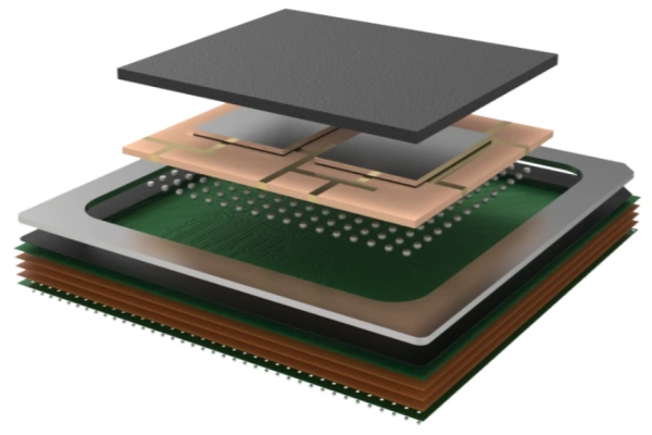
Abstract This article delves into the synergistic development of ultra-high-density packaging (SiP) and PCB design. It elaborates on the significance of their integration, explores the challenges and solutions in the [...]
In the field of electronic circuits, the impedance matching of SPI signal lines is of utmost importance, especially in high - speed application scenarios. SPI (Serial Peripheral Interface), as a [...]
TO TO (Transistor Outline) is a type of transistor package designed to allow the leads to be molded and used for surface mounting. It is primarily made of plastic and [...]