How to Choose PCB Core Materials
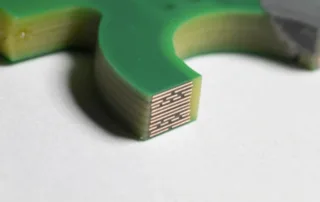
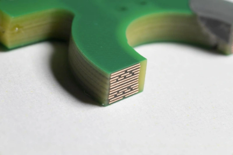
When a printed circuit board (PCB) maker gets a quote request for a multilayer design and the material instructions are missing or not clear, picking the PCB core thickness becomes [...]
Choosing the right PCBA (Printed Circuit Board Assembly) supplier isn’t just another procurement task—it’s a strategic decision that can directly influence your product quality, manufacturing timelines, brand reputation, and overall [...]
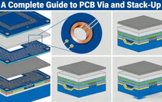
—Common Classifications of Vias— Through-holes are connection holes between the top and bottom layers of a PCB , and these holes also provide interconnection between internal PCB layers. Blind vias are vias that connect the surface [...]
Introduction: PCB plating processes require careful attention . It 's more than just applying a random layer of coating . First, it protects copper wires from oxidation . Copper easily oxidizes in air, which can easily lead [...]
How can we design to maximize yield, reduce costs, and shorten delivery? DFM (Design for Manufacturability) pitfalls in PCB design are a major cause of yield decline, cost increases, and [...]
For later component assembly and manual assembly, a PCB assembly drawing is made for component placement. Then the silkscreen reference designators are needed. Many new PCB designers adjust the silkscreen [...]
Electromagnetic Compatibility (EMC) is an important measure. It shows if electronic devices work well in an electromagnetic environment and do not cause problems for other devices. In PCB design, not [...]
hybrid In printed circuit board (PCB) making, drilling steps are a key part of both product function and production work. The trend toward smaller electronic devices shows more need for density [...]
I. PCB Surface Solder Mask Application Technology The solder mask layer constitutes a permanent dielectric coating in PCB manufacturing. Functionally, this layer prevents solder bridging during assembly, provides environmental protection [...]
Introduction In the vast landscape of Printed Circuit Board (PCB) manufacturing, Copper Clad Laminate (CCL) is the unsung hero, serving as the fundamental building block. CCL is a composite material, [...]
Symbols on PCB boards are divided into component symbols, electrical connection symbols, labeling and indication symbols, and special function symbols. These symbols carry crucial information for design, production, assembly, and [...]
In the highly competitive world of Printed Circuit Board (PCB) manufacturing, achieving zero defects is not just a lofty goal but a necessity for survival and success. At GreatPCB, we [...]