PCB Annular Ring Too Small? How to Fix Tight Through-Hole Pads

If a PCB annular ring is too small, first confirm the finished hole the connector needs. Measure the ring, hole-to-copper clearance, and copper-to-copper clearance separately. If enlarging the pad would violate copper spacing, check whether you can reroute the adjacent copper or move the connector and its footprint together.
In the worked example, the ring requires a pad diameter of at least 1.22 mm. The available copper gap allows no more than 1.20 mm. Those bounds explain why changing the diameter alone cannot solve the conflict.
Identify Which Clearance Rule Fails
In a plated through-hole (PTH), the annular ring is the copper land around the hole on a given layer. As the drill shifts relative to the pad, the ring narrows on one side. The hole touches the pad edge at tangency. It crosses that edge at breakout. Check whether the thin side is where the trace joins the pad, since that is where a breakout can interrupt the connection.
When a design rule check (DRC) flags a crowded connector, inspect the two features named in the error on the affected layer.
| Check | Measure between | What it tells you |
|---|---|---|
| Annular ring | The hole edge and the nearest edge of its own copper pad | How much land remains around the hole on that layer |
| Hole-to-copper clearance | The hole edge and the closest unrelated copper | How close the hole comes to a track, pad, or plane on another net |
| Copper-to-copper clearance | The pad edge and the closest unrelated copper edge | How closely the copper features approach each other |
A solder mask opening controls where copper is exposed for soldering. Changing the opening may address a mask or assembly issue. The underlying pad, hole, and copper gap retain their original dimensions. Check each affected copper layer because the nearest feature can be a different pad on the surface or a plane on an inner layer.
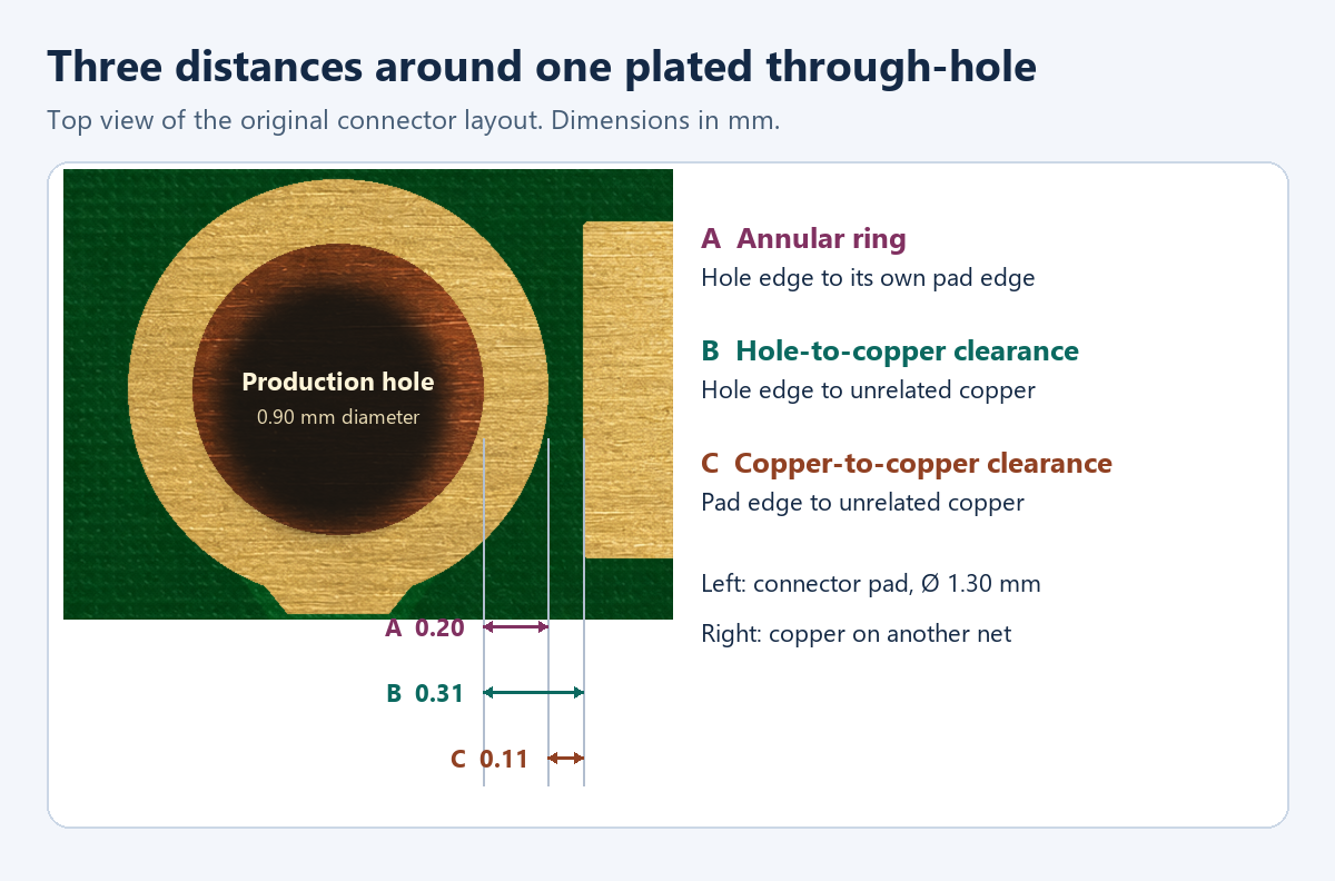
PCB macro illustration. Measurements A and B start at the production hole edge. Measurement C starts at the copper pad edge. All values are illustrative.
Calculate the Ring Using the Right Hole Size
Start with the connector drawing. Confirm the pin shape, maximum dimensions, positional tolerance, and any recommended hole pattern. For a round soldered pin, subtracting the maximum pin diameter from the minimum finished hole diameter gives a basic diametral fit check. In the example, a 0.65 mm maximum pin and a 0.80 ± 0.05 mm finished hole leave 0.10 mm of diametral clearance at the small end of the hole range. A multi-pin connector also has to fit across the whole pattern. For rectangular leads, slots, or press-fit contacts, use the applicable part and hole requirements. GreatPCB’s footprint guide
For a round, centered hole, subtract the applicable hole diameter from the pad diameter and divide by two. The diameter you use depends on the check:
| Check on a 1.30 mm copper pad | Hole diameter used | Calculated ring |
|---|---|---|
| Nominal geometry at the finished hole | 0.80 mm | 0.25 mm |
| Example production-tool geometry before plating | 0.90 mm | 0.20 mm |
The fabricator may drill a larger hole before plating so the finished opening meets the specified diameter. Confirm which diameter the fabricator uses for its CAM ring check and whether its rules already account for drill-to-copper registration on the affected layer. Apply any additional allowance only if the rule calls for it.
See What Happens When the Hole Moves Off Center
With the pad and tool diameters fixed at 1.30 mm and 0.90 mm, the centered ring is 0.20 mm. Move the hole center 0.08 mm and the thin side drops to 0.12 mm. The copper on the far side is wider, so a measurement taken only there would miss the problem.
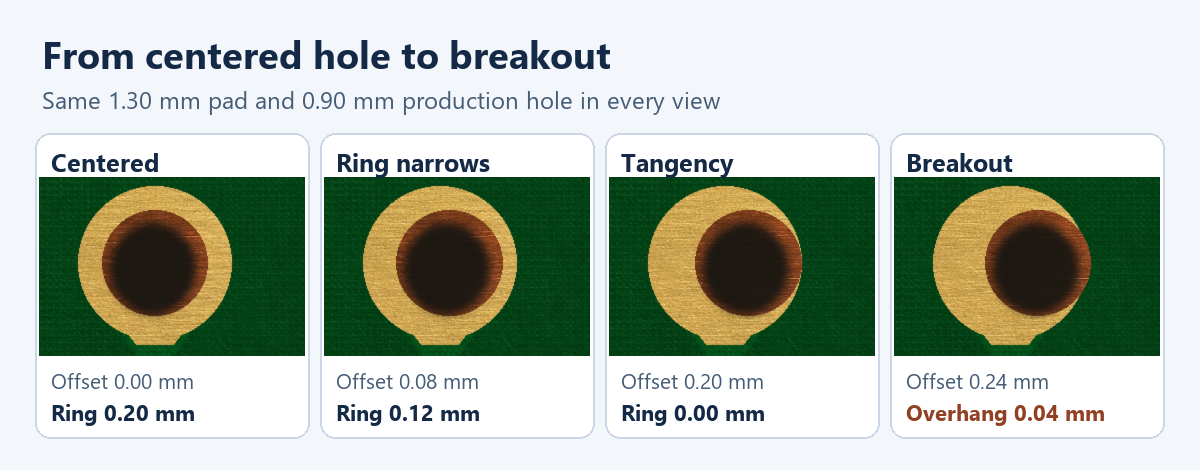
Four rendered views of the same pad. Follow its right edge as the hole shifts toward it.
For these two circles, minimum ring = centered ring − center offset while the hole remains inside the pad. At 0.20 mm of offset, the hole meets the pad edge. At 0.24 mm, it extends 0.04 mm beyond it. The chart continues below zero to show that overhang as a signed distance.
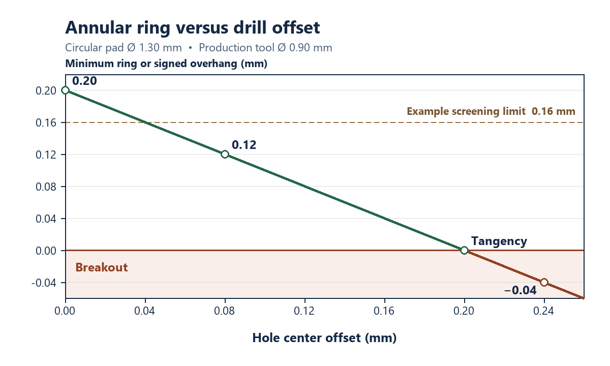
Each point matches a view above. The dashed line marks the example’s 0.16 mm screening limit, reached at 0.04 mm of offset, well before tangency. The plotted values are geometric distances. Actual breakout rates depend on the process and its registration variation.
Use the board shop’s rules to judge the remaining ring on each relevant layer. A planned hole offset also changes the lead position relative to its land pattern. A manufacturing registration error consumes copper margin around the intended position. For slots or noncircular pads, measure the closest edge along the actual outline instead of using the circular formula.
Fix a Tight Connector Footprint Without Losing Fit
In the original layout, the nearest unrelated copper edge is 0.76 mm from the center of the 1.30 mm pad. With the 0.90 mm production tool centered, the copper gap is 0.11 mm, while the hole-to-copper clearance is 0.31 mm. Those two readings lead to different decisions.
The table uses illustrative screening limits of 0.16 mm for the ring, 0.28 mm for hole-to-copper clearance, and 0.16 mm for copper spacing. The example compares nominal geometry. Production release calls for the actual process rules and tolerances.
Find Out Whether Changing the Pad Alone Can Work
With the hole and neighboring copper fixed, the two rules put opposite bounds on the pad diameter.
- Ring sets a minimum of 1.22 mm. Add twice the required 0.16 mm ring to the 0.90 mm tool diameter.
- Copper spacing sets a maximum of 1.20 mm. Subtract the required 0.16 mm gap from the 0.76 mm distance to the neighboring copper edge, then double the result.
The minimum exceeds the maximum. Every centered round pad at this location fails at least one of the two checks. Moving the neighboring edge 0.10 mm away raises the upper bound to 1.40 mm, so the original 1.30 mm pad fits. Hole-to-copper clearance is checked separately because it depends on the distance from the hole edge to the neighboring copper.
Compare the Layout Changes
| Layout change | Ring, min. | Hole to copper | Copper gap | Screening result |
|---|---|---|---|---|
| Original layout | 0.20 mm | 0.31 mm | 0.11 mm | Copper spacing fails |
| Shrink the pad diameter to 1.16 mm | 0.13 mm | 0.31 mm | 0.18 mm | Copper spacing passes. The ring fails. |
| Move the adjacent copper 0.10 mm away | 0.20 mm | 0.41 mm | 0.21 mm | All three pass |
| Move the connector and its footprint 0.10 mm away | 0.20 mm | 0.41 mm | 0.21 mm | All three pass locally. Check mechanical fit. |
| Move only the hole 0.08 mm toward the adjacent copper | 0.12 mm | 0.23 mm | 0.11 mm | All three fail. Pin alignment also needs review. |
For this layout, moving adjacent copper first preserves the verified hole pattern. If the copper belongs to a plane or a constrained route, check the electrical effect of rerouting it. If you can move the connector, check the mating position, enclosure, and the rest of its pins before accepting the local clearance result.
A different pad shape can create space in one direction. Measure the remaining land around the hole and review the exposed solderable area with the assembler. A teardrop adds copper at the trace-to-pad junction, so recheck the spacing around the added copper and the ring on the other sides. If the part geometry leaves too little room, compare a different connector footprint or confirm a suitable process with the fabricator.
Send the Fabricator a Clear DFM Question
Point the fabricator to the connector reference, affected pad or slot, and copper layer. Include the component drawing, finished hole dimensions and tolerance, plating requirement, and the two copper features causing the conflict. Ask what production tool it would use, what ring and hole-to-copper clearances apply, and whether the design needs a change before release. GreatPCB’s design-for-manufacturing guide
Once you agree on the geometry, apply the rules to the board, regenerate the manufacturing outputs, and inspect the affected layers. If this is an update to an existing board, compare the new package with the one the factory previously received. How to compare PCB revisions before manufacturing
Table of Contents
Related Posts
PCBA Prototype
October 23, 2026
PCBA Prototype
October 19, 2026