
How to Compare PCB Revisions Before Manufacturing
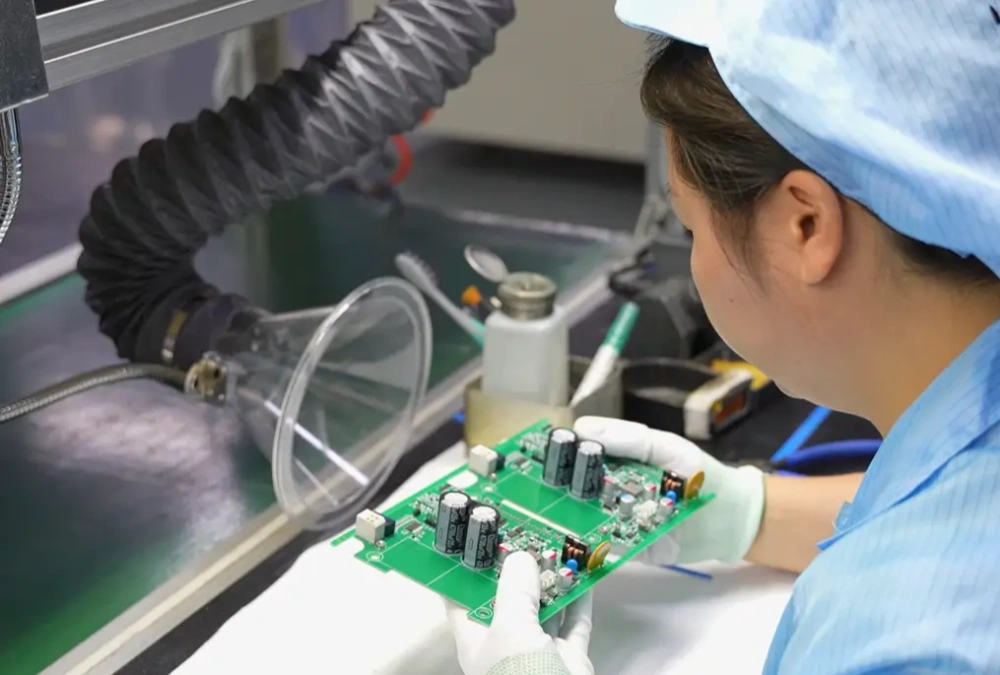
The Rev B Gerbers show the new USB-C footprint. In the same ZIP, the BOM still lists the old part number for J1. The bare board could arrive with the new footprint while the assembly team orders the old connector.
To catch a mismatch like this, start with the last package the factory received and the approved change list. Compare the exported Gerbers and drill data, then check that the BOM, placement file, and assembly drawing describe the intended build.
Start With the Last Released Files and the Approved Change List
Use the actual Rev A package sent to the factory as your baseline. Keep it separate from the Rev B package you intend to send. If the product has several assembly variants, confirm which one each package describes. Re-exporting an older design can introduce differences through changed output settings or copper pours, which makes it harder to identify what changed in Rev B. Altium’s manufacturing file review guide
List what the change should affect before opening the comparison tool. In this simplified example, Rev B uses a different USB-C connector at J1. Its footprint pads and plated mounting holes move. An unrelated copper feature stays in place. The approved BOM changes from the example part number DEMO-A to DEMO-B. The example uses the same placement coordinates and rotation for both connectors. On your board, check these against the new footprint and mechanical drawing.
If you are releasing a board for the first time, inspect the complete output package. For a major redesign, compare only the regions or features with a useful baseline and review the new outputs on their own.
Compare Gerber Files and Drill Data Layer by Layer
Check Alignment Within Each Revision
Open the exported files from each ZIP. Verify the layer assignments, copper layer order, and board outline. Match layers by function before comparing the two versions. If filenames changed, confirm the mapping against the layer attributes or the fabrication drawing.
In each revision, overlay the drill data on the corresponding copper and board outline. Check that holes land where the design calls for them. Use at least two widely separated reference features where available to spot a translation, scaling, or orientation problem. For a separate NC drill file, verify its units, coordinate interpretation, and origin. Confirm plated and non-plated hole information and slot dimensions where they matter to the change. Altium’s fabrication output documentation
Compare the Same Layers Across Revisions
Toggle between matching layers or use a two-color overlay. If your viewer offers an XOR view, it highlights areas occupied in only one of the two images. Return to the individual views when you need to identify which revision contains a feature. Measure suspect dimensions against the approved drawing or the fabricator’s requirements. FAB 3000 comparison example
For J1, check the changed copper pads and mounting holes. Then inspect the associated solder mask and paste openings if the footprint change affects them. Check the clearances that matter to the connector, including the board edge or enclosure interface. Finally, scan layers and areas that the change list says should stay the same.
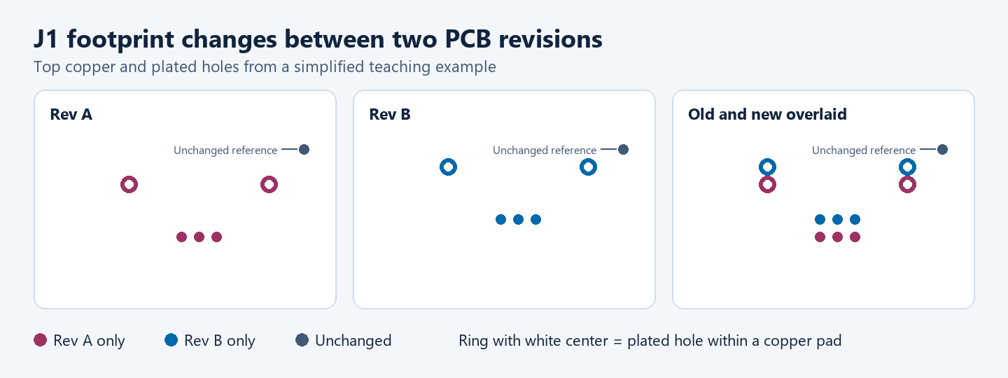
The simplified overlay shows J1’s old and new pad and hole positions. The dark reference feature stays in the same place in both versions.
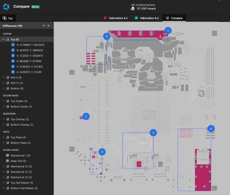
Altium 365 Gerber Compare highlights differences between matching layers. Screenshot from Altium’s manufacturing file review guide.
Decide Which Differences Need Action
A difference view shows where the artwork changed. Use the approved change list to decide whether each change belongs there. A wide band of highlights around the board can mean a coordinate mismatch. A small highlight at J1 can be a genuine clearance problem. Start with how the differences are distributed.
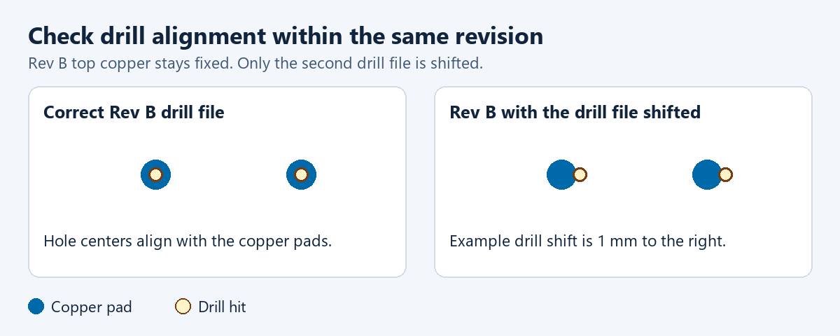
Both views use the same Rev B copper. Changing only the drill file shifts the hole centers while the copper pads stay in place.
| What you see | What to check | When to hold the release |
|---|---|---|
| The whole board appears shifted between versions. | Check the import units, origin, and orientation. Compare the outline and stable features far apart. | Hold if you cannot reconcile the coordinate systems or if files within the proposed ZIP disagree. |
| Only the holes appear shifted. | Overlay the holes and copper from the same revision. Check drill export and import settings. In the example, shifting only the drill file 1 mm in X moves the holes off the centers of their pads. | Hold if the drill file and copper still disagree after you verify the settings. Correct the source or export, then regenerate and check the affected files. |
| Copper changes outside the J1 area. | Review the source layout, copper repour, and output settings. Check whether changes to clearances or connectivity are intended. Where supported, compare a CAM-extracted netlist with the approved design netlist. | Hold when the change has no approved explanation or its effect is unresolved. |
| The rendered layers match, but the files differ. | Check whether the change is in comments, attributes, or other file content. Verify any changed attributes that affect layer identification or interpretation. | Hold if the metadata describes the wrong layer or leaves the intended manufacturing data ambiguous. |
A layout design-rule check covers the source design. The release review checks the exported files the factory will use. Apply the relevant drawing requirements and DFM checks where the difference affects manufacturability. Altium’s guidance on inspecting fabrication outputs · Ucamco’s Gerber format overview
Catch Assembly Files From the Old Revision
Use the same reference designator across the released assembly documents. A BOM row can group several parts under one number, so find J1 in the reference list and confirm the approved manufacturer part number for the intended assembly variant. In the placement file, check the board side, position, and rotation against the approved layout and the assembler’s convention. Use the assembly drawing to confirm the location, orientation, and any notes that apply to J1. PCB BOM guide · Pick and place file guide
| File in the Rev B ZIP | What you find in the example | Decision |
|---|---|---|
| Gerber and drill files | The new pads and holes match the expected geometry. | The example geometry check passes. |
| Placement file | J1’s approved placement coordinates and rotation are unchanged. | The placement row can remain as it is. |
| BOM | J1 still lists DEMO-A. The approved part is DEMO-B. | Hold the ZIP and correct the BOM. |
The geometry and placement results can both pass while the wrong connector is still on the purchasing list. Use the approved BOM to resolve the mismatch. In your release records, identify which revision of each document belongs to the build. The bare board, BOM, and assembly drawing may each have their own revision number.
Release the Exact ZIP You Reviewed
After correcting a file, reopen the ZIP you plan to send. Check the board number and assembly variant, verify the approved combination of files, and confirm that each difference has been explained or corrected. For the J1 example, the corrected archive shows DEMO-B in the BOM and the same accepted copper, drill, and placement data. Keep the sent package with its change and approval records so the next revision starts from a known baseline.
If your fabricator provides production data for approval, compare it with the package you sent and record any agreed CAM changes. That review checks the factory’s prepared data after your own release comparison. For the next stage, use the PCB pilot build checklist to identify what the revised assembly needs to prove. Eurocircuits’ production data comparison guide
Table of Contents
Related Posts
PCBA Prototype
November 13, 2026
PCBA Prototype
November 13, 2026
